
This technical article was updated on July 23, 2020.
In the first two parts of my ADC accuracy series, I established the differences between resolution and accuracy for an analog-to-digital converter (ADC) and explained the factors that contribute to total unadjusted error (TUE) of the ADC. Most of these errors are static errors that can be calibrated under ambient conditions. System performance can continue to drift even after calibration, however, due to a change in temperature, which is common in many factory automation and control and other applications. Other factors such as aging of electronic components, humidity and pressure can also play a role in long-term performance drift.
Three major components affect accuracy drift in a data-acquisition system:
- ADC offset drift
- ADC gain drift
- Voltage reference drift
The mismatch between the internal resistors, capacitors, switches and other active devices will affect the offset and gain drift of an ADC. ADC offset drift (TDOS) is sometimes also referred to as bipolar zero-error drift, especially in the case of converters that can handle bipolar input ranges. The entire transfer function of the ADC shifts in either direction as a consequence of the offset drift, as shown in Figure 1. TDOS is not at all impacted by the drift of the voltage reference.
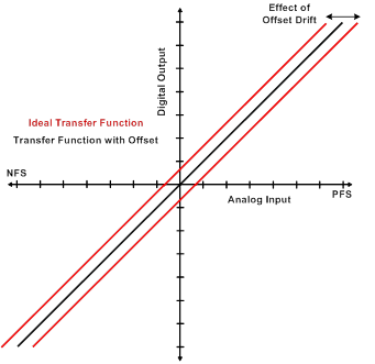
Figure 1: Effect of offset drift
On the other hand, ADC gain drift (TDG) is largely affected by reference drift. Thus, it is often specified with external reference and the measurement procedure compensates for the effects of reference drift. The entire transfer function of the ADC rotates around the bipolar zero in either direction as a consequence of the gain drift, as shown in Figure 2.
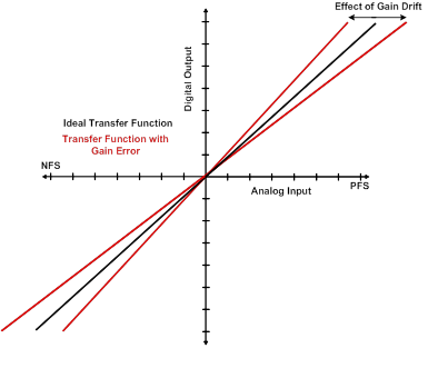
Figure 2: Effect of gain drift
Voltage reference drift (internal or external) is a major contributor to the overall accuracy of the data-acquisition signal chain. Typically, the external reference sources exhibit much better temperature drift performance compared to the integrated references. The reference voltage directly impacts the ADC transfer function, so any change in this voltage changes the slope of the ADC transfer function proportionally. This is nothing but gain error.
The overall gain of the ADC is a function of the reference voltage along with a multiplication factor, K. This multiple factor varies from device to device. For example, the maximum input range of the ADS8688 varies from -2.5*VREF to +2.5*VREF, so the full-scale range (FSR) is equal to 5*VREF. If the reference exhibits a temperature drift equal to TDREF ppm/⁰C, then the overall change in the slope of ADC transfer function is equal to 5*TDREF ppm/⁰C.
If a data-acquisition system is calibrated under an ambient temperature of TA and the system temperature varies from TLO to THI, then Equation 1 denotes the total error (TDERR) due to drift over the entire temperature range. Note that drift is always a bipolar specification.
TDERR = K*TDREF*(THI, TLO – TA)MAX + TDG*(THI, TLO – TA)MAX + TDOS*(THI, TLO – TA)MAX (Equation 1)
For example, if you’re using a device like the ADS8688 in a system with a temperature variation from 0⁰C to 80⁰C and performing calibration at 25⁰C, then the worst-case error for a ±10.24V input range can be calculated as 3135ppm (Equation 2). This corresponds to an accuracy of 0.3% and is mainly dominated by the temperature drift of the internal reference.
TDERR = 5*10*55 + 4*55 + 3*55 = 3135ppm (Equation 2)
Some systems may be sensitive to inaccuracy because of such large temperature variations. In those cases, a commonly used method to calibrate for temperature drift is to measure the gain and offset error of the entire signal chain at different temperatures and record the calibration factors into a look-up table. This is obviously a time-consuming process and also requires additional hardware to accurately measure the temperature. Both tasks also translate into additional system cost.
For systems that do not perform temperature calibration, it is important to pay attention to the drift specifications in order to calculate and budget for the worst-case error based on Equation 1. It is important to know the statistical worst-case drift of devices under varying process conditions for such systems. Most manufacturers usually specify drift as a typical specification to save cost, but this is not very useful for system designers. Hence, devices like the ADS8688 – which specify worst-case gain, offset and reference temperature drift specifications – make it easier for system designers to budget for the worst-case system accuracy over the entire operating temperature range.
Having reached the conclusion of this three-part series, you should have an understanding of the various factors that affect the DC accuracy of an ADC signal chain and optimize your system design for temperature drift performance.
You can learn more about how to optimize precision ADC performance in your control system by reading the SAR ADC Response Times blog series by my colleague Kaustubh Gadgil.
Additional resources:
- See the ADS8688 successive approximation register (SAR) ADC with 16 bits, eight channels, 500kSPS and bipolar inputs off +5V supply.
- SLAA587: Read the application report: “ADC Performance Parameters – Convert the Units Correctly!”
- TIDA-00170: See the SAR ADC accuracy principles in action in a 16-bit analog mixed-input and output module for programmable logic controllers (PLCs).
Get common A/D conversion and other board- and system-level design formulas at your fingertips with the Analog Engineer’s Pocket Reference.