

Bad communication is a common problem engineers face with their analog-to-digital converters (ADCs). While this isn’t strictly a data converter issue, it does come up regularly and can be hard to debug. In this post I’ll talk about how to debug digital communication problems, along with some things you might see when communications go wrong.
A picture is worth a thousand words
If you can’t communicate with the device or if the communication doesn’t make sense, get an oscilloscope capture of the communication lines. If the device uses serial peripheral interface (SPI), it helps to use a four-channel oscilloscope. Capture the C͞S, SCLK, DIN and DOUT/D͞R͞D͞Y lines. If the device uses I2C, capture SDA and SCL and check that you are using the correct I2C address.
Communications should match the timing characteristics in the data sheet. See that the clock rates aren’t too fast, that the pulse widths aren’t too narrow, that the setup and hold times are observed, and that the waveforms are clean and well behaved. Figure 1 shows an example of SPI timing characteristics.
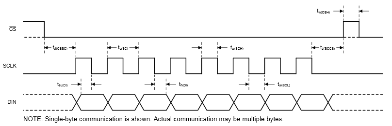
Figure 1: Serial interface timing diagram from the ADS1220
With a scope shot, you can even read the bits coming out of the device. You can confirm reads and writes directly, without having the microcontroller interpret the results. If the scope shot doesn’t match what you read on the computer, then the source code may have an error. The error could be a wrong command coming from the microprocessor or missing bytes from a universal serial bus (USB) interface.
We just don’t speak the same language
One common error is the version of SPI communication being used. For those more experienced with analog circuits instead of digital communications, this is a common mix-up. As a quick overview, there are four versions of SPI dealing with clock polarity (CPOL) and phase (CPHA).
Many of TI’s delta-sigma ADCs use CPOL=0, CPHA=1, where the SCLK dwells low and the DIN and DOUT are clocked at the falling edge of SCLK. Data is set up with the rising edge of SCLK. Figure 2 shows a sample readout of SPI data.

Figure 2: SPI communication using CPOL=0, CPHA=1
I don’t know if you heard me correctly
Another important debugging tool is the read back of all registers in the device. This helps when the part is doing something you don’t understand. If your system requires a microcontroller to set up the device, the code may not be sending what you think it’s sending. In that case, it helps to ensure that the write was correct by reading back the configuration status.
It’s too loud in this room
Noise in the communication lines may cause serious error. In particular, noise on the SCLK is a big problem. When there is extra noise on SCLK, the device might think that the SPI has clocked another bit of data, advancing the data being clocked out or clocked in without warning.
If there is noise causing an extra SCLK, an extra added SCLK may force DOUT high (or DOUT/D͞R͞D͞Y high if the two lines are combined) at the end of clocking out the data. In some devices, two extra SCLKs may force a calibration cycle. This varies from device to device and may not always be the case. However, if the DOUT/D͞R͞D͞Y is forced high more often than not, or if you see an unexplained calibration cycle in scope shots, these clues may be used to help debug the problem.
Don’t interrupt me when I’m talking
Clocking out the data shouldn’t be done asynchronously to ADC conversions. The D͞R͞D͞Y line indicates when new data are available and updated on DOUT. When D͞R͞D͞Y transitions from high to low, new data can be clocked out with SCLK and must be clocked out before the next D͞R͞D͞Y indication. If the data-read operation does not complete before the D͞R͞D͞Y is indicated again, the device does not retain the remaining data on DOUT. Instead, DOUT is updated while being clocked out – resulting in corrupted data. If you simply clock out data without trying to detect the D͞R͞D͞Y output, you may be reading invalid data. Figure 3 shows an instance where the data being read is interrupted by a new D͞R͞D͞Y indication after the sixth SCLK, shown by the arrow. The ADC thinks that the seventh SCLK is the start of a new data read.
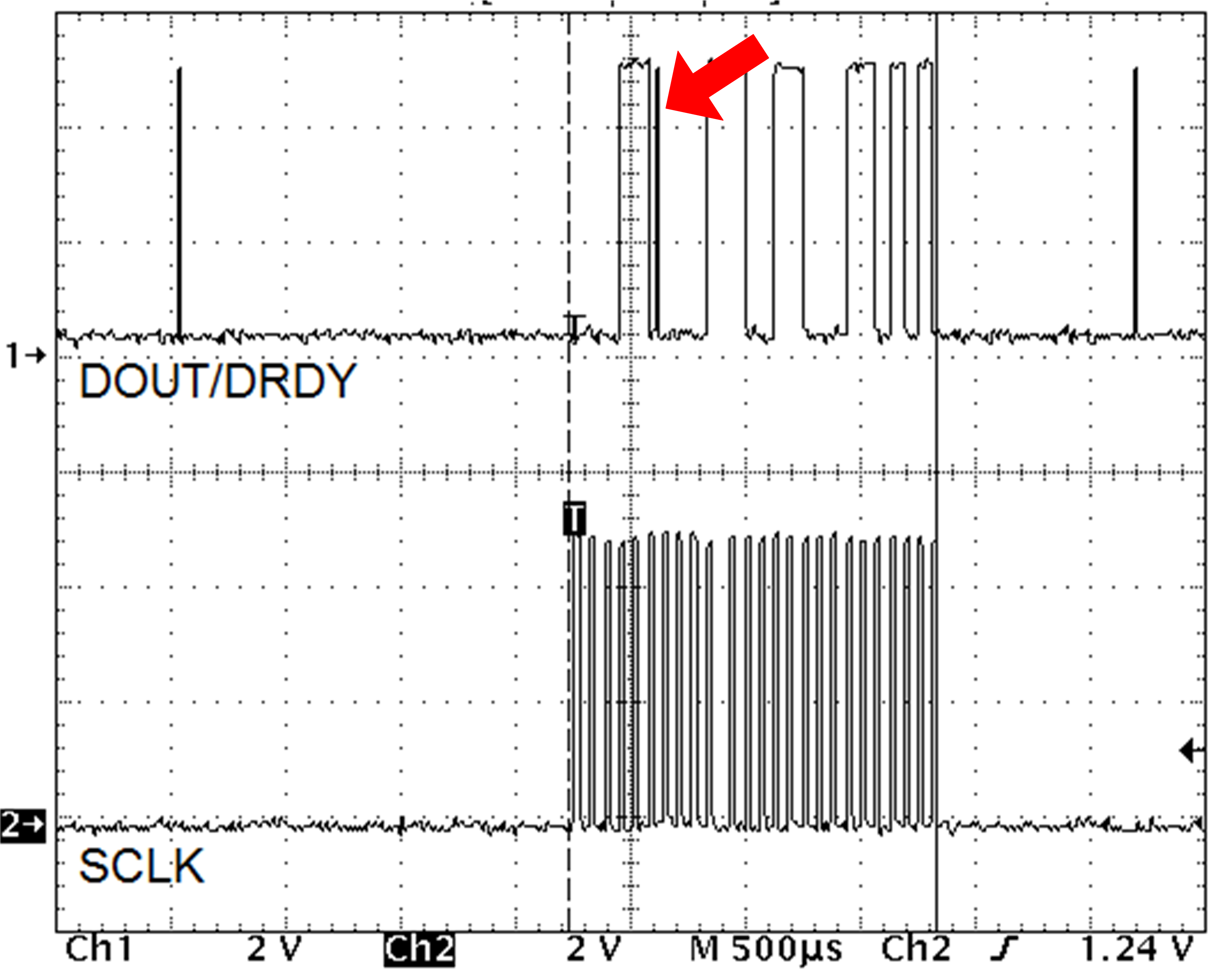
Figure 3: The ADC read is interrupted by a D͞R͞D͞Y indication
Did you say what I think you said?
It helps to know what you are expecting as a conversion result. Apply a known voltage to the inputs and a known reference voltage and collect some data. You may need to measure back the inputs and reference, but the output data should match what you expect for the conversion. Examining raw data from the device is better than the converted data you get from the microcontroller.
I hear you loud and clear
These are a few common errors made in communicating with products in the precision data-converter line. By knowing what kinds of problems can arise and by doing some simple debugging, you can avoid common communication errors.
Related blogs: Delta-sigma ADC basics: Walking around the delta-sigma blocks
- Delta Sigma ADC Basics: Understanding the delta-sigma modulator
- On Board with Bonnie: ADC noise from the inside out
- Best of Baker's Best -- Precision Data Converters, Delta-Sigma ADCs
Additional resources:
Small Form Factor, 2-Wire 4 to 20mA Current Loop RTD Temperature Transmitter Reference Design