

This technical article was updated on July 23, 2020.
Designing high-performance multiplexed data-acquisition (DAQ) systems with high throughputs can be difficult. That’s because the entire system, shown in Figure 1, only has up to the maximum time between conversions of the analog-to-digital converter (ADC) to settle within one-half of a least significant bit (LSB). For example, if the ADC is operating at a 1-MSPS throughput, the system must settle in less than 1µs; but for a robust design, it is best to have the system settle to one-half LSB in 500ns. Choosing the settling time to be 1µs would not give you any extra time for variation in component specifications, temperature drift, process shift or aging over the product’s life – and would likely result in error.
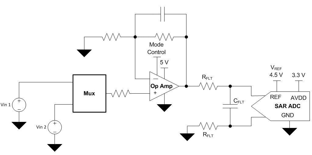
Figure 1: Multiplexed DAQ system
In order to understand the tight time constraint on the settling time, let’s go through an example of what’s occurring during the acquisition and conversion periods of the ADC. Figure 2 shows a simplified schematic of what’s inside the ADS8860.
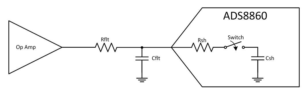
Figure 2: ADS8860 internal simplified schematic
Figure 3 shows a timing diagram of the system with the ADS8860 operating at 1MSPS. During the acquisition period (ACQ) of the ADC, the switch in Figure 2 is closed and the sample and hold capacitor, CSH, charges to the voltage at the input of the ADC. Once the acquisition period ends, the conversion period (CONV) begins.
During conversion, the switch is open and the ADC converts the voltage that CSH was charged to during acquisition into a digital value. Therefore, if the system does not settle to the proper voltage before conversion starts, shown by the red line in Figure 3, CSH will not charge to the correct voltage, resulting in a conversion error.
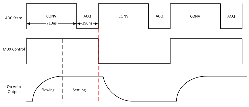
Figure 3: System timing diagram
Choosing the correct operational amplifier (op amp) to drive the SAR ADC will help optimize system performance. The op amp needs to have excellent AC performance, such as low total harmonic distortion (THD), low noise, fast settling time, high slew rate and a high gain bandwidth (GBW).
The low THD and noise specifications are important so that the op amp does not degrade the performance of the ADC. The high GBW, fast settling time, and high slew rate are most important when trying to achieve fast settling. The high slew rate and fast settling time are necessary because you want a fast, large signal step with minimal ringing. If the op amp has a slow slew rate and a long settling time, it will take a long time for the large signal to transition to the final voltage and a long time for the small signal to settle within the desired error band.
An op amp that meets all of the criteria I’ve described is the OPA625. The OPA625 has a GBW of 120MHz, a slew rate of 115V/µs, 16-bit settling with a 4V step of 280ns, voltage noise of 2.5nV/, and a THD specification of -135dB at 10kHz. All of these specifications make the OPA625 to drive an ideal SAR ADC and achieve the fast settling requirements for a high-performance multiplexed DAQ system.
Check back in a couple of weeks where I will talk about the circuit configuration for driving the ADS8860 with the OPA625; how the requirements to drive the ADS8860 effect stability; and finally, measured data showing the OPA625 settling to one-half LSB in 500ns while driving the ADS8860.
Related resources:
- Download datasheets for the ADS8860 and OPA625.
- Watch on-demand training courses on slew rate, settling time and more in TI Precision Labs – Op Amps.
- For more information on how a successive approximation (SAR) ADC operates, check out the blog post, “SAR ADC response times: Interface topology makes a difference.”
- To learn more about slew rate and settling time, check out the courses offered in our on-demand training series, TI Precision Labs – Op Amps.
