

This post is co-authored by Raphael Puzio.
Photodiode-based light sensing is a common application of operational amplifiers (op amps) used in medical equipment, industrial automation, robotics, point-of-sale machines, drones, smoke detectors and building automation equipment. This blog demonstrates how to build a cost-sensitive, accurate photodiode circuit.
A photodiode sensor produces a current proportional to the light level presented to it. Depending on the application, the photodiode is operated in either a photovoltaic or photoconductive mode; each has its own merits, which Bruce Trump discussed in detail in this post from his blog, The Signal.
Most applications operate the photodiode in photoconductive mode, with an op amp in a transimpedance configuration to amplify the current. In photoconductive mode, the photodiode is held at a zero-volt (Figure 1a) or reverse voltage bias (Figure 1b), preventing it from forward biasing.
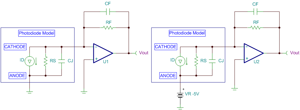
Figure 1: Photodiode in photoconductive mode with zero-volt bias (a); or reverse-voltage bias (b)
Equation 1 calculates the direct current (DC) transfer function for the circuits shown in Figure 1 (note that the photodiode current (iD) is flowing away from the op-amp inverting node):

The three-step process outlined in John Caldwell’s series on transimpedance amplifiers (see part 3, “What op amp bandwidth do I need?”) determines the minimum required op-amp gain bandwidth for transimpedance configurations. The minimum bandwidth is based on the required transimpedance gain and signal bandwidth, along with the total capacitance presented to the inverting node of the op amp. The diode capacitance often dominates the inverting-node capacitance, but don’t forget to include the effects of the op-amp input capacitance. We summarized the three steps explained in John’s posts here for quick reference.
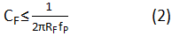
1. Choose the maximum feedback capacitance (CF) based on the feedback resistor (RF) and the signal -3dB bandwidth (fP) (Equation 2):
 2. Calculate the total capacitance (CIN) at the inverting input of the amplifier. For the circuits shown in Figure 1, this is equal to Equation 3:

where CJ is the diode junction capacitance, CD is the op-amp differential input capacitance and CCM2 is the op-amp inverting input common-mode input capacitance.
3. Calculate the minimum required op-amp gain bandwidth product (fGBW) (Equation 4):

By following these three simple steps, you can avoid many of the stability and performance issues commonly associated with transimpedance amplifier circuits by selecting an amplifier with sufficient bandwidth to perform the required transimpedance gain at the desired signal bandwidth.
Along with meeting bandwidth requirements, the op amp must also meet the system’s DC accuracy requirements. The most important DC specification in many transimpedance applications is the input bias current (iB) of the op amp. iB will directly sum or subtract with the input signal current, which can cause large errors depending on the magnitude of iB compared to the signal current.
The example shown in Figure 2 uses a 5MΩ resistor to apply a 5MV/A gain to a 100nA full-scale input current. With the input bias current set to 0A, the full-scale output voltage is 500mV – which is expected based on the transfer function in Equation 1. The circuit on the right in Figure 2 displays the effects of the same circuit with an op amp iB of 10nA. In this case, the output voltage is 450mV, which shows that the 10nA input bias current caused a 50mV (or 10%) error from the ideal 500mV output signal.
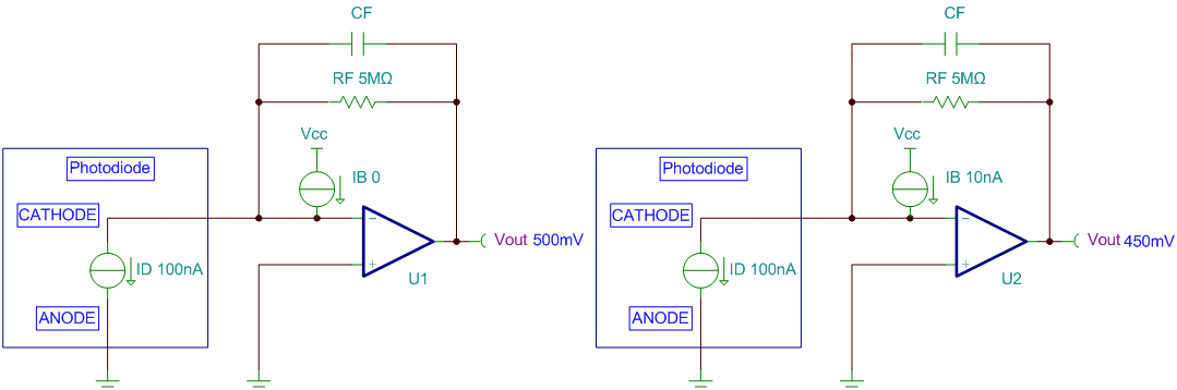
Figure 2: Input bias current effects in transimpedance amplifier circuits
Equation 5 calculates the percentage error of the full-scale range (%FSR) based on the full-scale input current (iIN_FS) and the op amp’s iB:

The TLV600x devices are a new family of high-performance general-purpose amplifiers for a wide variety of cost-conscious transimpedance applications, such as consumer drones, POS machines, smoke detectors and building automation equipment. The key features that make the TLV600x great for transimpedance applications is the wide bandwidth of 1MHz, low typical input bias currents of 1pA and a low input capacitance of 6pF total. Other beneficial features are a low quiescent current of 100µA maximum, rail-to-rail input and output swings, and low current and voltage noise densities of 5fA/√Hz and 28nV/√Hz, respectively.
Table 1 lists different transimpedance gain and bandwidth combinations for the TLV600x based on Equations 1 through 4. Be sure to keep the total input capacitance below the maximum input capacitance (CIN_MAX) to avoid stability issues.
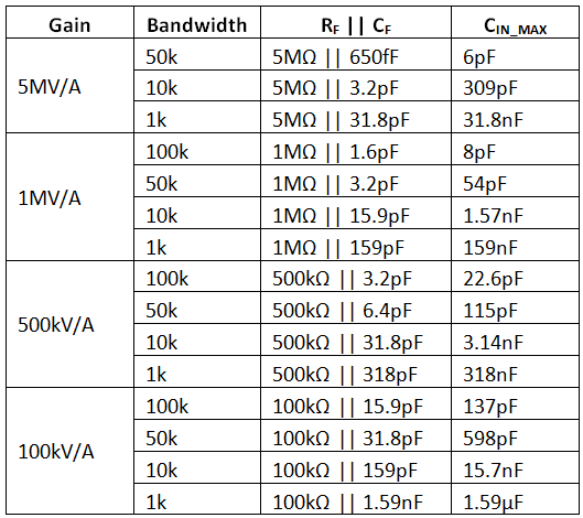
Note: fGBW is 1MHz, CD is 1pF and CCM is 5pF for the TLV600x.
Table 1: Quick design calculator for TLV600x transimpedance applications
Figure 3 shows the simulated step-response results for a 1MV/A gain and 50kHz bandwidth with the maximum 54pF of input capacitance from the photodiode. The output overshoot and ringing are minimal, indicating a stable design.
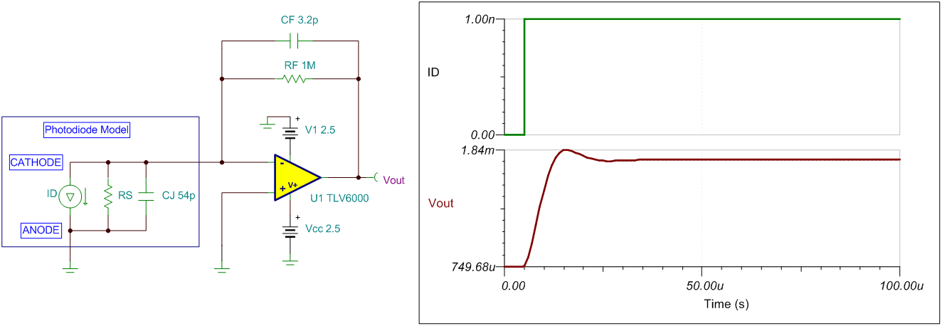
Figure 3: TLV6000 step-response results; gain = 1MV/A, bandwidth = 50kHz
Many applications use op amps in the transimpedance configuration to amplify low-level currents. Designing the transimpedance circuit can be simplified to a few easy steps. First, follow the three steps from John’s blog posts to select the required op-amp bandwidth. Then sort the remaining results to find a device with an iB specification that meets the system’s DC requirements.
Do you have questions about transimpedance op-amp designs? Log in and leave a comment below letting us know your experience with transimpedance configurations or any questions you have.
Additional resources
- Find commonly used analog design formulas in the “Analog Engineer’s Pocket Reference” e-book.
- Read the other two parts in John Caldwell’s three-part blog series on transimpedance circuits:
- See TI’s portfolio of performance op amps for cost-conscious applications.
