

Do you feel like your adjustable voltage regulator deserves some margin? I do, and I have some good news: all it takes is one DAC and one resistor!
The traditional feedback system for a linear regulator (LDO), shown in Figure 1, has a resistor divider network from the voltage output to the feedback pin and then to ground. Choosing these resistor values determines the output of the regulator.
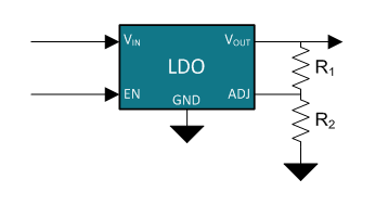
Figure 1: Common implementation of adjustable LDO feedback
Figure 2 shows the topology of a typical adjustable LDO. Notice that the internal reference of the LDO feeds to the non-inverting terminal of the amplifier, which drives the gate of the pass FET. Hooking up the inverting input of the amplifier to the feedback (FB) or adjust (ADJ) pin of the LDO then creates a feedback loop. This causes the amplifier to drive the gate of the pass FET in such a way that the resistor divider of R1 and R2 develops a voltage at the FB pin equal to the LDO’s internal reference voltage.

Figure 2: Example LDO topology, TPS7A7002
However, this is a static solution. If your circuit encounters ohmic losses on a high-current dynamic load or if you’re implementing dynamic voltage scaling, for instance, your circuit might require “reprogramming” of the output voltage from the regulator. Traditionally, this isn’t possible without physically replacing the resistors. Adding a DAC and resistor to the circuit, however, as shown in Figure 3, will allow you to raise and lower the output voltage of the regulator on the fly by programming the DAC voltage.
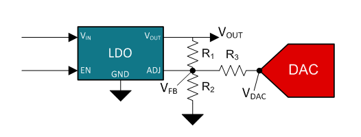
Figure 3: Adjustable LDO feedback with a precision DAC
After choosing the regulator and DAC that you would like to use, there are a few pieces of information you need to gather or select before designing this circuit, described in Table 1.
Table 1: Circuit design parameters
Consider the currents going in and out of the VFB node shown in Figure 3, which is connected to the ADJ pin of the LDO. Almost no current flows in or out the device through the ADJ pin (on the order of 0.01µA). As I previously mentioned, the output voltage of the LDO is always produced such that the voltage at the ADJ pin – and therefore the VFB node – is equal to the LDO’s internal reference voltage. Thus, the current through R2 is constant. It follows that any sourcing or sinking of current by the DAC through R3 is reflected as a proportional voltage increase or decrease at VOUT to compensate for the changing current that must flow through R1. This helps write the relationship between the two remaining unknowns, R1 and R3, based on Figure 3 and expressed as Equation 1:

Equation 1 shows that the total amount of current change through R3 due to the DAC output voltage has to be equal to current change through R1 by varying the output voltage of the regulator. Equation 2 is the sum of the currents in and out of the VFB node based on Figure 3:

Here, VDAC is the output voltage of the DAC reflected in Figure 3. To have VNOM as the regulator output when the DAC voltage is at VDACN, you can substitute these design parameters from Table 1 in for VOUT and VDAC, respectively. The VFB node will always be regulated to the voltage of the LDO internal reference, so you can substitute VREF for VFB to get Equation 3:

You can use Equations 1 and 3 to calculate the remaining two resistor values. As an example, I’ve chosen the values shown in Table 2 based on a DAC with an output range of 0V to 2.5V and an LDO with an internal reference of 1.246V.

Table 2: Example circuit design parameters
Plugging values from Table 2 into Equation 1 yields the following relationship between R1 and R3:

Substituting 2.5R1 for R3 into Equation 3 – along with the other circuit design parameters that you have chosen – and then solving will give you the value of R1:

Finally, you can reuse the result to find the value of R3 from R1:

Now your design is done. Building the results of this exercise in TINA-TI™ software confirms that the design is working as expected. At mid scale of the DAC, the voltage is at the nominal 5V, while at the full and zero scale the voltage is at 4.5V and 5.5V, respectively. Figure 4 shows the schematic used, while Figure 5 shows the simulation results.
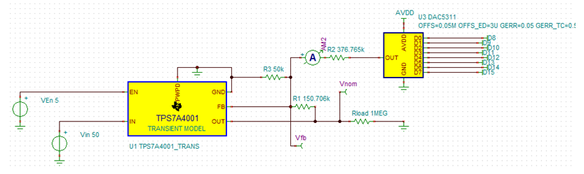
Figure 4: TINA-TI™ schematic of circuit design

Figure 5: Simulation results of circuit design
TI’s DAC5311, DAC6311 and DAC7311 are 8-/10-/12-bit voltage output DACs that have output buffers and are very low power. Be careful not to choose an unbuffered DAC. The output amplifier needs to both sink and source current.
For the purpose of this explanation, I used an LDO as the example. The same margining principles apply for margining a switching regulator as well.
In my next post, I will talk about how to effectively margin, monitor and control a whole system of regulators with one device. To be notified about my next post and other technical how-to posts on Precision Hub, click the subscribe button on this post to log in and subscribe.
Additional resources
- Need more advice on designing with LDOs? Check out posts on the Power House Blog.
- Search for solutions, get help and solve problems in the TI E2E™ Precision Data Converter Forum.
- For more resources about working with Precision DACs, visit the Precision DAC Learning Center.
