In the first two posts of the delta-sigma (ΔΣ) analog-to-digital converter (ADC) basics blog series, we have discussed the two basic building blocks used in ΔΣ ADCs: the modulator and the digital filter. You’ll encounter many other integrated circuits as you work with these devices, however. The available functional blocks and the many variations of each one are why there are so many different ΔΣ ADCs customized to particular applications.
In this post, I’ll briefly look at many of these functions and talk about how they fit into different applications. Let’s imagine each type of ΔΣ ADC as a neighborhood, and walk around some block diagrams, beginning in a sparsely populated rural area.
ADS1252 (rural)
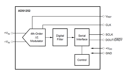
Figure 1 shows the block diagram of the ADS1252 ΔΣ ADC. The modulator and digital filter are the essential parts. Let’s look at the other represented blocks.
Figure 1: Block diagram of the ADS1252 ΔΣ ADC
Interface and control logic
The interface and control logic blocks are common to all ΔΣ ADCs and represent all that is needed to complete the device. In the case of the ADS1252, a simple two-pin interface (SCLK and DOUT/DRDY) provides an output of the conversion results. This basic interface is what allows the ADS1252 to quickly start up and provide data from a wide variety of sensors. Meanwhile, the logic controls can synchronize conversions with multiple devices, notify you when a data conversion is complete and power down the ADC when not in use.
Rural areas are usually quiet and devoid of the daily hustle-and-bustle of urban life. Similarly, the ADS1252 is an unsophisticated and simple ΔΣ ADC, that can be used for process control applications and thermocouple measurements.
Now that you’re familiar with the basic ΔΣ ADC block diagram, let’s walk toward a nearby town …
ADS1259 (suburb)
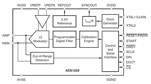
On our stroll into town, we pass through a suburb. The houses are getting closer and closer together, although each one is still unique. It is here where we encounter the ADS1259, shown in Figure 2. Check out all the blocks!
Figure 2: Block diagram of the ADS1259 ΔΣ ADC
Internal reference
All ΔΣ ADCs require a voltage reference to define the full-scale range of the modulator. The ADS1259 block diagram shows an integrated 2.5V reference. In most applications, the integrated reference provides sufficient input range and noise performance (more on reference noise in a future blog post); however, input pins (VREFP and VREFN) still allow for the application of an external reference. An external reference is usually required when performing ratiometric measurements (more on ratiometric measurements in a future post).
Internal oscillator (clock generator)
All ΔΣ ADCs use a clock source to determine the modulator’s sampling rate. The ADS1259’s clock-generator block provides a clock without any external components; however, attaching an external crystal may help stabilize the modulator clock or generate a different modulator clock frequency, affecting the modulator sampling rate and output data rates.
While the suburban homes are still fairly dispersed, we simply haven’t the time to see everything in the area. Similarly, the ADS1259 has many other features that I won’t cover in this post; you can learn more about them here. Devices like the ADS1259 integrate many useful circuits into the ADC to significantly reduce the amount of printed circuit board (PCB) area and cost required to fit a ΔΣ ADC into a system. However, even with the high level of integration, we are left with plenty of flexibility to use this device in many different applications, including high-resolution weigh scales. The facade of the ADS1259 might not make it obvious, but it is one of the lowest-noise, highest-resolution ΔΣ ADCs used for DC measurements.
ADS1220 (urban)
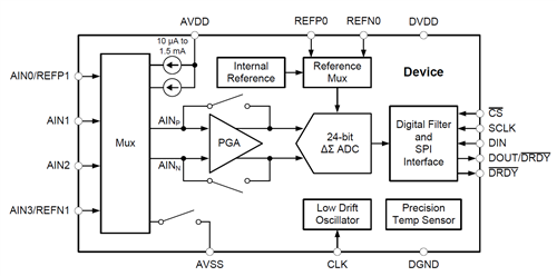
We finally reach town and find this urban area to be a little more crowded, much like the ADS1220 block diagram shown in Figure 3.
Figure 3: Block diagram of the ADS1220 ΔΣ ADC
Multiplexer
The multiplexer increases the number of ADC inputs and allows for measurements of multiple sensor signals consecutively. To measure multiple sensors simultaneously, multiple ΔΣ ADCs or multiple ΔΣ modulators would be necessary (see the ADS1278 block diagram for an example). There are also ΔΣ ADCs with much larger channel counts (see the ADS1258 block diagram).
Programmable gain amplifier (PGA)
A PGA placed before the ΔΣ modulator amplifies small signals, providing higher resolution (more on gain and resolution in a future post).
IDACs
You can use programmable current digital-to-analog converter (IDAC) sources to excite and measure most resistive-type sensors such as thermistors, resistance temperature detectors (RTDs) and strain gauges.
You can find almost anything in a crowded city; likewise, the ADS1220 contains nearly everything you’d need to interface directly to a sensor. This ADC is well suited for instrumentation using temperature or bridge (strain) sensors and is ideal for space-constrained or low-power designs like temperature and pressure transmitters.
The road goes on and on, but it is here where our journey ends; we’ll part ways (for now). I hope you are more comfortable navigating ΔΣ ADC block diagrams. If you’d like for me to cover a particular functional block I didn’t include, let me know in the comments below.
For more in-depth information, see the following resources:
- Use the Precision ADC parametric search tool to search for the right ADC for your application.
- Browse questions about TI’s precision ADC applications in the TI E2E™ Community Precision Data Converters forum.
- See the ADS1220 delta-sigma ADCin these precision designs in the TI Designs reference design library:
- Temperature Sensor Interface Module for Programmable Logic Controllers (TIDA-00018)
- Small Form Factor, 2-Wire 4 to 20mA Current Loop RTD Temperature Transmitter Reference Design (TIDA-00165)


-

gvs t
-
Cancel
-
Up
0
Down
-
-
Reply
-
More
-
Cancel
Comment-

gvs t
-
Cancel
-
Up
0
Down
-
-
Reply
-
More
-
Cancel
Children