This thread has been locked.

If you have a related question, please click the "Ask a related question" button in the top right corner. The newly created question will be automatically linked to this question.

CC2340R5: how can i verify 32K on CC2340R5

Expert 1085 points
Part Number: CC2340R5

Hi Experts.

Any chip on the previous CCXXX2 agama platform,
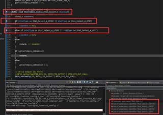
We all use the following program to do 32K test.

    //IOCPortConfigureSet(20, IOC_PORT_AON_CLK32K, IOC_STD_OUTPUT);
    //AONIOC32kHzOutputEnable();
    //while(1);

But in CC2340 SDK, there seems to be no AONIOC32kHzOutputEnable function.
Is there any change in the 32K test method in CC2340? Can you tell me how to test 32K in CC2340.

Thanks.

  • Hi,

    To verify the clock on the CC23XX platform, you will need to follow a different method. You can output the clock onto a GPIO and measure the GPIO externally to verify the frequency of the clock signal.

    The following functions should output the low frequency clock onto a GPIO:

    uint8_t gLfTickToGpio_enabled = 0;
    static void LftickToGpio_dtb5_dio24_enable()
    {
        if (gLfTickToGpio_enabled)
            return;
        else
            gLfTickToGpio_enabled = 1;
    
        // DIO24 can be driven by DTB5
        const uint8_t dtb_bit = 5;
        const uint8_t dio = 24;
        const uint8_t dsel_lftick = 13; // LFTICK is bit 4
    
        // drive output low first
        GPIO_setConfig(IOC_O_IOC24, GPIO_CFG_OUTPUT | GPIO_CFG_OUT_LOW);
    
        // Configure the IOC.IOC24.PORTCFG MMR to select DTB
        HWREG(IOC_BASE + IOC_O_IOC24) &= ~IOC_IOC24_PORTCFG_M;
        HWREG(IOC_BASE + IOC_O_IOC24) |= IOC_IOC24_PORTCFG_DTB;
    
        // Select the DTB mux selects in IOC (and if required in source clock IP) in such a way that zero is driven on DTB0
        //         Example: Configure IOC.DTBCFG.ULLSELL = 1 to select CKM DTB0
        // ULLSEL mux select (select CKM)
        HWREG(IOC_BASE + IOC_O_DTBCFG) &= ~IOC_DTBCFG_ULLSEL_M;
        HWREG(IOC_BASE + IOC_O_DTBCFG) |= 0x1 << IOC_DTBCFG_ULLSEL_S; // 0x1 to route CKM (CKMDIG) to DTB0 (DTB bit 0)
    
        // Enable IOC.DTBOE.EN5
        HWREG(IOC_BASE + IOC_O_DTBOE) &= ~IOC_DTBOE_EN5_M;
        HWREG(IOC_BASE + IOC_O_DTBOE) |= IOC_DTBOE_EN5_EN;
    
        // Step 1: select 5-bit signal group to output on DTB[5:1]
        HWREG(CKMD_BASE + CKMD_O_DTBCTL) &= ~CKMD_DTBCTL_DSEL0_M;
        HWREG(CKMD_BASE + CKMD_O_DTBCTL) |= dsel_lftick << CKMD_DTBCTL_DSEL0_S;
    
        // Step 2: Configure CKMD.DTBCTL.EN=1 for Enabling DTB output
        // enable DTB output
        HWREG(CKMD_BASE + CKMD_O_DTBCTL) &= ~CKMD_DTBCTL_EN_M;
        HWREG(CKMD_BASE + CKMD_O_DTBCTL) |= CKMD_DTBCTL_EN;
    }
    
    static void LftickToGpio_dtb5_dio24_disable()
    {
        // Enable IOC.DTBOE.EN5
        HWREG(IOC_BASE + IOC_O_DTBOE) &= ~IOC_DTBOE_EN5_M;
        gLfTickToGpio_enabled = 0;
    }

    To enable this functionality, you can use the following functions:

    uint8_t gXtalToGpio_isEnabled = 0;
    static void XtalToGpio_enable(Xtal_Select_e xtalType)
    {
        uint8_t clockSrc;
    
        if (xtalType == Xtal_Select_e_HFOSC || xtalType == Xtal_Select_e_HFXT)
        {
            clockSrc = 0xC;
        }
        else if (xtalType == Xtal_Select_e_LFOSC || xtalType == Xtal_Select_e_LFXT)
        {
            clockSrc = 0x7;
        }
        else
        {
            return; // invalid
        }
    
        if (gXtalToGpio_isEnabled)
        {
            return;
        }
        else
        {
            gXtalToGpio_isEnabled = 1;
        }
    
        // drive output low first
        GPIO_setConfig(DTB0_DIO_ID, GPIO_CFG_OUTPUT | GPIO_CFG_OUT_LOW);
    
        // Configure the IOC.IOC19.PORTCFG MMR to select DTB
        HWREG(IOC_BASE + IOC_O_IOC19) &= ~IOC_IOC19_PORTCFG_M;
        HWREG(IOC_BASE + IOC_O_IOC19) |= IOC_IOC19_PORTCFG_DTB;
    
        // Select the DTB mux selects in IOC (and if required in source clock IP) in such a way that zero is driven on DTB0
        //         Example: Configure IOC.DTBCFG.ULLSELL = 1 to select CKM DTB0
        // ULLSEL mux select (select CKM)
        HWREG(IOC_BASE + IOC_O_DTBCFG) &= ~IOC_DTBCFG_ULLSEL_M;
        HWREG(IOC_BASE + IOC_O_DTBCFG) |= 0x1 << IOC_DTBCFG_ULLSEL_S; // 0x1 to route CKM (CKMDIG) to DTB0 (DTB bit 0)
    
    
        // Enable IOC.DTBOE.EN0
        HWREG(IOC_BASE + IOC_O_DTBOE) &= ~IOC_DTBOE_EN0_M;
        HWREG(IOC_BASE + IOC_O_DTBOE) |= IOC_DTBOE_EN0_EN;
    
        // Select the DTB mux selects in IOC (and if required in source clock IP) in such a way that clock is driven on DTB0
        // Example: Step 1: Configure CKMD.DTBCTL.CLKSEL = 0xA for HFOSC
        // select which clock (CKMD) to output on DTB0 (DTB[0])
        HWREG(CKMD_BASE + CKMD_O_DTBCTL) &= ~CKMD_DTBCTL_CLKSEL_M;
        HWREG(CKMD_BASE + CKMD_O_DTBCTL) |= (clockSrc) << CKMD_DTBCTL_CLKSEL_S;
        // Step 2: Configure CKMD.DTBCTL.EN=1 for Enabling DTB output
        // enable DTB output
        HWREG(CKMD_BASE + CKMD_O_DTBCTL) &= ~CKMD_DTBCTL_EN_M;
        HWREG(CKMD_BASE + CKMD_O_DTBCTL) |= CKMD_DTBCTL_EN;
    }
    static void XtalToGpio_disable()
    {
        if (!gXtalToGpio_isEnabled)
        {
            return;
        }
    
        // Disable IOC.DTBOE.EN0
        HWREG(IOC_BASE + IOC_O_DTBOE) &= ~IOC_DTBOE_EN0_M;
    
        gXtalToGpio_isEnabled = 0;
    }

    Best Regards,

    Jan

  • Hi Jan,

    thanks for your response.

    I have reviewed the functions LftickToGpio_dtb5_dio24_enable and XtalToGpio_enable, which utilize dio24 and dio19 respectively.

    Q1: Does LftickToGpio_dtb5_dio24_enable call this, and then call XtalToGpio_enable?

    Q2: What is the primary purpose of dio19 within the XtalToGpio_enable function?

    Q3:Can this DIO19 be changed to another DIO? We use a 4X4 package, and the chip does not have DIO19.

    Thanks.

  • Hi,

    My apologies for any confusion.

    Q1: Does LftickToGpio_dtb5_dio24_enable call this, and then call XtalToGpio_enable?

    The XtalToGpio_enable() is used to enable outputting a clock to a GPIO (and specifying which clock to enable). The LftickToGpio_dtb5_dio24_enable() is used drive the output of the crystal to the gpio.

    Q2: What is the primary purpose of dio19 within the XtalToGpio_enable function?

    I believe that has to do with the mux settings to get the output of the crystal.

    Q3:Can this DIO19 be changed to another DIO? We use a 4X4 package, and the chip does not have DIO19.

    I would need to look into this. In the meantime, can you clarify if you are using a LaunchPad or a customboard?

    Best Regards,

    Jan

  • Q3:Can this DIO19 be changed to another DIO? We use a 4X4 package, and the chip does not have DIO19.

    I would need to look into this. In the meantime, can you clarify if you are using a LaunchPad or a customboard?

    >>>>>>>>

    Hi Jan, Thanks for your response.

    We use custom board,

    We are TI third-party supplier.

    so we designed a small-size module using a 4X4 package.

    could you help me confirm the above question?

    Thanks.

  • Hi,

    Based on some initial research, I think you should be able to change to DIO16, DIO20, DIO21, or DIO24 instead of DIO19. I would try DIO24 to start.

    Best Regards,

    Jan

  • Hi Jan,

    I appreciate your help, I encountered a compilation error, I searched the SDK all over the world, but I couldn't find these types, can you give me more information?

    I want to test 32K, can I directly assign clockSrc to 0x07 directly?

    like this.

    uint8_t gXtalToGpio_isEnabled = 0;
    static void XtalToGpio_enable(/*Xtal_Select_e xtalType*/)
    {
        uint8_t clockSrc;
    
        /*if (xtalType == Xtal_Select_e_HFOSC || xtalType == Xtal_Select_e_HFXT)
        {
            clockSrc = 0xC;
        }
        else if (xtalType == Xtal_Select_e_LFOSC || xtalType == Xtal_Select_e_LFXT)
        {
            clockSrc = 0x7;
        }
        else
        {
            return; // invalid
        }*/
        clockSrc = 0x7;//add by weli
    
        if (gXtalToGpio_isEnabled)
        {
            return;
        }
        else
        {
            gXtalToGpio_isEnabled = 1;
        }
    
        // drive output low first
        //GPIO_setConfig(DTB0_DIO_ID, GPIO_CFG_OUTPUT | GPIO_CFG_OUT_LOW);
        GPIO_setConfig(24, GPIO_CFG_OUTPUT | GPIO_CFG_OUT_LOW);
    
        // Configure the IOC.IOC19.PORTCFG MMR to select DTB
        HWREG(IOC_BASE + IOC_O_IOC19) &= ~IOC_IOC19_PORTCFG_M;
        HWREG(IOC_BASE + IOC_O_IOC19) |= IOC_IOC19_PORTCFG_DTB;
    
        // Select the DTB mux selects in IOC (and if required in source clock IP) in such a way that zero is driven on DTB0
        //         Example: Configure IOC.DTBCFG.ULLSELL = 1 to select CKM DTB0
        // ULLSEL mux select (select CKM)
        HWREG(IOC_BASE + IOC_O_DTBCFG) &= ~IOC_DTBCFG_ULLSEL_M;
        HWREG(IOC_BASE + IOC_O_DTBCFG) |= 0x1 << IOC_DTBCFG_ULLSEL_S; // 0x1 to route CKM (CKMDIG) to DTB0 (DTB bit 0)
    
    
        // Enable IOC.DTBOE.EN0
        HWREG(IOC_BASE + IOC_O_DTBOE) &= ~IOC_DTBOE_EN0_M;
        HWREG(IOC_BASE + IOC_O_DTBOE) |= IOC_DTBOE_EN0_EN;
    
        // Select the DTB mux selects in IOC (and if required in source clock IP) in such a way that clock is driven on DTB0
        // Example: Step 1: Configure CKMD.DTBCTL.CLKSEL = 0xA for HFOSC
        // select which clock (CKMD) to output on DTB0 (DTB[0])
        HWREG(CKMD_BASE + CKMD_O_DTBCTL) &= ~CKMD_DTBCTL_CLKSEL_M;
        HWREG(CKMD_BASE + CKMD_O_DTBCTL) |= (clockSrc) << CKMD_DTBCTL_CLKSEL_S;
        // Step 2: Configure CKMD.DTBCTL.EN=1 for Enabling DTB output
        // enable DTB output
        HWREG(CKMD_BASE + CKMD_O_DTBCTL) &= ~CKMD_DTBCTL_EN_M;
        HWREG(CKMD_BASE + CKMD_O_DTBCTL) |= CKMD_DTBCTL_EN;
    }

  • Hi Jan

    I compiled the program, but I can't see the 32K square wave on DIO20 or DIO24.

    /*
     *  ======== main_freertos.c ========
     */
    #include <stdint.h>
    
    #ifdef __ICCARM__
        #include <DLib_Threads.h>
    #endif
    
    /* POSIX Header files */
    #include <pthread.h>
    
    /* RTOS header files */
    #include <FreeRTOS.h>
    #include <task.h>
    
    #include <ti/drivers/Board.h>
    
    #include <ti/devices/DeviceFamily.h>
    #include DeviceFamily_constructPath(driverlib/dbell_regs.h)
    
    #include DeviceFamily_constructPath(inc/hw_types.h)
    #include DeviceFamily_constructPath(inc/hw_memmap.h)
    #include DeviceFamily_constructPath(inc/hw_ioc.h)
    #include DeviceFamily_constructPath(inc/hw_ckmd.h)
    
    #include <ti/drivers/Power.h>
    #include <ti/drivers/power/PowerCC23X0.h>
    #include <ti/drivers/Temperature.h>
    #include <ti/drivers/GPIO.h>
    extern void *mainThread(void *arg0);
    
    /* Stack size in bytes */
    #define THREADSTACKSIZE   2048
    
    
    uint8_t gLfTickToGpio_enabled = 0;
    static void LftickToGpio_dtb5_dio24_enable()
    {
        if (gLfTickToGpio_enabled)
            return;
        else
            gLfTickToGpio_enabled = 1;
    
        // DIO24 can be driven by DTB5
        const uint8_t dtb_bit = 5;
        const uint8_t dio = 24;
        const uint8_t dsel_lftick = 13; // LFTICK is bit 4
    
        // drive output low first
        //GPIO_setConfig(IOC_O_IOC24, GPIO_CFG_OUTPUT | GPIO_CFG_OUT_LOW);
        GPIO_setConfig(24, GPIO_CFG_OUTPUT | GPIO_CFG_OUT_LOW);
    
        // Configure the IOC.IOC24.PORTCFG MMR to select DTB
        HWREG(IOC_BASE + 24) &= ~IOC_IOC24_PORTCFG_M;
        HWREG(IOC_BASE + 24) |= IOC_IOC24_PORTCFG_DTB;
    
        // Select the DTB mux selects in IOC (and if required in source clock IP) in such a way that zero is driven on DTB0
        //         Example: Configure IOC.DTBCFG.ULLSELL = 1 to select CKM DTB0
        // ULLSEL mux select (select CKM)
        HWREG(IOC_BASE + IOC_O_DTBCFG) &= ~IOC_DTBCFG_ULLSEL_M;
        HWREG(IOC_BASE + IOC_O_DTBCFG) |= 0x1 << IOC_DTBCFG_ULLSEL_S; // 0x1 to route CKM (CKMDIG) to DTB0 (DTB bit 0)
    
        // Enable IOC.DTBOE.EN5
        HWREG(IOC_BASE + IOC_O_DTBOE) &= ~IOC_DTBOE_EN5_M;
        HWREG(IOC_BASE + IOC_O_DTBOE) |= IOC_DTBOE_EN5_EN;
    
        // Step 1: select 5-bit signal group to output on DTB[5:1]
        HWREG(CKMD_BASE + CKMD_O_DTBCTL) &= ~CKMD_DTBCTL_DSEL0_M;
        HWREG(CKMD_BASE + CKMD_O_DTBCTL) |= dsel_lftick << CKMD_DTBCTL_DSEL0_S;
    
        // Step 2: Configure CKMD.DTBCTL.EN=1 for Enabling DTB output
        // enable DTB output
        HWREG(CKMD_BASE + CKMD_O_DTBCTL) &= ~CKMD_DTBCTL_EN_M;
        HWREG(CKMD_BASE + CKMD_O_DTBCTL) |= CKMD_DTBCTL_EN;
    }
    
    static void LftickToGpio_dtb5_dio24_disable()
    {
        // Enable IOC.DTBOE.EN5
        HWREG(IOC_BASE + IOC_O_DTBOE) &= ~IOC_DTBOE_EN5_M;
        gLfTickToGpio_enabled = 0;
    }
    
    uint8_t gXtalToGpio_isEnabled = 0;
    static void XtalToGpio_enable(/*Xtal_Select_e xtalType*/)
    {
        uint8_t clockSrc;
    
        /*if (xtalType == Xtal_Select_e_HFOSC || xtalType == Xtal_Select_e_HFXT)
        {
            clockSrc = 0xC;
        }
        else if (xtalType == Xtal_Select_e_LFOSC || xtalType == Xtal_Select_e_LFXT)
        {
            clockSrc = 0x7;
        }
        else
        {
            return; // invalid
        }*/
        clockSrc = 0x7;//add by weli
    
        if (gXtalToGpio_isEnabled)
        {
            return;
        }
        else
        {
            gXtalToGpio_isEnabled = 1;
        }
    
        // drive output low first
        //GPIO_setConfig(DTB0_DIO_ID, GPIO_CFG_OUTPUT | GPIO_CFG_OUT_LOW);
        GPIO_setConfig(20, GPIO_CFG_OUTPUT | GPIO_CFG_OUT_LOW);
    
        // Configure the IOC.IOC19.PORTCFG MMR to select DTB
        HWREG(IOC_BASE + IOC_O_IOC20) &= ~IOC_IOC20_PORTCFG_M;
        HWREG(IOC_BASE + IOC_O_IOC20) |= IOC_IOC20_PORTCFG_DTB;
    
        // Select the DTB mux selects in IOC (and if required in source clock IP) in such a way that zero is driven on DTB0
        //         Example: Configure IOC.DTBCFG.ULLSELL = 1 to select CKM DTB0
        // ULLSEL mux select (select CKM)
        HWREG(IOC_BASE + IOC_O_DTBCFG) &= ~IOC_DTBCFG_ULLSEL_M;
        HWREG(IOC_BASE + IOC_O_DTBCFG) |= 0x1 << IOC_DTBCFG_ULLSEL_S; // 0x1 to route CKM (CKMDIG) to DTB0 (DTB bit 0)
    
    
        // Enable IOC.DTBOE.EN0
        HWREG(IOC_BASE + IOC_O_DTBOE) &= ~IOC_DTBOE_EN0_M;
        HWREG(IOC_BASE + IOC_O_DTBOE) |= IOC_DTBOE_EN0_EN;
    
        // Select the DTB mux selects in IOC (and if required in source clock IP) in such a way that clock is driven on DTB0
        // Example: Step 1: Configure CKMD.DTBCTL.CLKSEL = 0xA for HFOSC
        // select which clock (CKMD) to output on DTB0 (DTB[0])
        HWREG(CKMD_BASE + CKMD_O_DTBCTL) &= ~CKMD_DTBCTL_CLKSEL_M;
        HWREG(CKMD_BASE + CKMD_O_DTBCTL) |= (clockSrc) << CKMD_DTBCTL_CLKSEL_S;
        // Step 2: Configure CKMD.DTBCTL.EN=1 for Enabling DTB output
        // enable DTB output
        HWREG(CKMD_BASE + CKMD_O_DTBCTL) &= ~CKMD_DTBCTL_EN_M;
        HWREG(CKMD_BASE + CKMD_O_DTBCTL) |= CKMD_DTBCTL_EN;
    }
    static void XtalToGpio_disable()
    {
        if (!gXtalToGpio_isEnabled)
        {
            return;
        }
    
        // Disable IOC.DTBOE.EN0
        HWREG(IOC_BASE + IOC_O_DTBOE) &= ~IOC_DTBOE_EN0_M;
    
        gXtalToGpio_isEnabled = 0;
    }
    
    /*
     *  ======== main ========
     */
    int main(void)
    {
        pthread_t           thread;
        pthread_attr_t      attrs;
        struct sched_param  priParam;
        int                 retc;
    
        /* initialize the system locks */
    #ifdef __ICCARM__
        __iar_Initlocks();
    #endif
        Board_init();
        Temperature_init();
    
        uint32_t hftrackctl =  HWREG( CKMD_BASE + CKMD_O_HFTRACKCTL );
    
        /* ==== /ti/drivers/Power initialization ==== */
        Power_setConstraint(PowerLPF3_DISALLOW_IDLE);
        Power_setConstraint(PowerLPF3_DISALLOW_STANDBY);
    
        /* High performance clock buffer enable */
        HWREG( CKMD_BASE + CKMD_O_HFXTCTL ) |= ( CKMD_HFXTCTL_HPBUFEN | CKMD_HFXTCTL_EN );
    
        /* Enable tracking loop */
        HWREG( CKMD_BASE + CKMD_O_HFTRACKCTL ) = hftrackctl | CKMD_HFTRACKCTL_EN;
    
        /* Initialize the attributes structure with default values */
        pthread_attr_init(&attrs);
    
        /* Set priority, detach state, and stack size attributes */
    
        LftickToGpio_dtb5_dio24_enable();
        XtalToGpio_enable();
        while(1);
    
        priParam.sched_priority = 1;
        retc = pthread_attr_setschedparam(&attrs, &priParam);
        retc |= pthread_attr_setdetachstate(&attrs, PTHREAD_CREATE_DETACHED);
        retc |= pthread_attr_setstacksize(&attrs, THREADSTACKSIZE);
        if (retc != 0) {
            /* failed to set attributes */
            while (1) {}
        }
    
        retc = pthread_create(&thread, &attrs, mainThread, NULL);
        if (retc != 0) {
            /* pthread_create() failed */
            while (1) {}
        }
    
        /* Start the FreeRTOS scheduler */
        vTaskStartScheduler();
    
        retur

  • Hi,

    My apologies for any confusion, this is the entire code used on our testing. We implemented it on a nortos gpiostandby project:

    /*
     * Copyright (c) 2022, Texas Instruments Incorporated
     * All rights reserved.
     *
     * Redistribution and use in source and binary forms, with or without
     * modification, are permitted provided that the following conditions
     * are met:
     *
     * *  Redistributions of source code must retain the above copyright
     *    notice, this list of conditions and the following disclaimer.
     *
     * *  Redistributions in binary form must reproduce the above copyright
     *    notice, this list of conditions and the following disclaimer in the
     *    documentation and/or other materials provided with the distribution.
     *
     * *  Neither the name of Texas Instruments Incorporated nor the names of
     *    its contributors may be used to endorse or promote products derived
     *    from this software without specific prior written permission.
     *
     * THIS SOFTWARE IS PROVIDED BY THE COPYRIGHT HOLDERS AND CONTRIBUTORS "AS IS"
     * AND ANY EXPRESS OR IMPLIED WARRANTIES, INCLUDING, BUT NOT LIMITED TO,
     * THE IMPLIED WARRANTIES OF MERCHANTABILITY AND FITNESS FOR A PARTICULAR
     * PURPOSE ARE DISCLAIMED. IN NO EVENT SHALL THE COPYRIGHT OWNER OR
     * CONTRIBUTORS BE LIABLE FOR ANY DIRECT, INDIRECT, INCIDENTAL, SPECIAL,
     * EXEMPLARY, OR CONSEQUENTIAL DAMAGES (INCLUDING, BUT NOT LIMITED TO,
     * PROCUREMENT OF SUBSTITUTE GOODS OR SERVICES; LOSS OF USE, DATA, OR PROFITS;
     * OR BUSINESS INTERRUPTION) HOWEVER CAUSED AND ON ANY THEORY OF LIABILITY,
     * WHETHER IN CONTRACT, STRICT LIABILITY, OR TORT (INCLUDING NEGLIGENCE OR
     * OTHERWISE) ARISING IN ANY WAY OUT OF THE USE OF THIS SOFTWARE,
     * EVEN IF ADVISED OF THE POSSIBILITY OF SUCH DAMAGE.
     */
    
    /*
     *  ======== pinStandby.c ========
     */
    #include <unistd.h>
    
    /* Driver Header files */
    #include <ti/drivers/GPIO.h>
    
    /* Example/Board Header files */
    #include "ti_drivers_config.h"
    
    #include DeviceFamily_constructPath(inc/hw_types.h)
    #include DeviceFamily_constructPath(inc/hw_memmap.h)
    #include DeviceFamily_constructPath(inc/hw_ckmd.h)
    #include DeviceFamily_constructPath(inc/hw_ioc.h)
    #include DeviceFamily_constructPath(inc/hw_pmctl.h)
    
    
    #define DTB0_DIO_ID   19
    typedef enum
    {
        Xtal_Select_e_HFOSC,
        Xtal_Select_e_LFOSC,
        Xtal_Select_e_HFXT,
        Xtal_Select_e_LFXT,
    } Xtal_Select_e;
    
    static void XtalToGpio_enable(Xtal_Select_e xtalType);
    static void XtalToGpio_disable();
    
    static void LftickToGpio_dtb5_dio24_enable();
    static void LftickToGpio_dtb5_dio24_disable();
    
    /*
     *  ======== mainThread ========
     */
    void *mainThread(void *arg0)
    {
        uint32_t standbyDuration = 5;
    
        /* Configure LED pins */
        GPIO_setConfig(CONFIG_GPIO_0, GPIO_CFG_OUTPUT | GPIO_CFG_OUT_LOW);
        GPIO_setConfig(CONFIG_GPIO_1, GPIO_CFG_OUTPUT | GPIO_CFG_OUT_HIGH);
    
        XtalToGpio_enable(Xtal_Select_e_HFXT);
        LftickToGpio_dtb5_dio24_enable();
        while (1);
    
        while (1)
        {
            XtalToGpio_enable(Xtal_Select_e_LFOSC);
            LftickToGpio_dtb5_dio24_enable();
            sleep(1);
            XtalToGpio_disable();
            LftickToGpio_dtb5_dio24_disable();
            sleep(1);
        }
    
    }
    
    uint8_t gXtalToGpio_isEnabled = 0;
    static void XtalToGpio_enable(Xtal_Select_e xtalType)
    {
        uint8_t clockSrc;
    
        if (xtalType == Xtal_Select_e_HFOSC || xtalType == Xtal_Select_e_HFXT)
        {
            clockSrc = 0xC;
        }
        else if (xtalType == Xtal_Select_e_LFOSC || xtalType == Xtal_Select_e_LFXT)
        {
            clockSrc = 0x7;
        }
        else
        {
            return; 
        }
    
        if (gXtalToGpio_isEnabled)
        {
            return;
        }
        else
        {
            gXtalToGpio_isEnabled = 1;
        }
    
        // drive output low first
        GPIO_setConfig(DTB0_DIO_ID, GPIO_CFG_OUTPUT | GPIO_CFG_OUT_LOW);
    
        // Configure the IOC.IOC19.PORTCFG MMR to select DTB
        HWREG(IOC_BASE + IOC_O_IOC19) &= ~IOC_IOC19_PORTCFG_M;
        HWREG(IOC_BASE + IOC_O_IOC19) |= IOC_IOC19_PORTCFG_DTB;
    
        // Select the DTB mux selects in IOC (and if required in source clock IP) in such a way that zero is driven on DTB0
        //         Example: Configure IOC.DTBCFG.ULLSELL = 1 to select CKM DTB0
        // ULLSEL mux select (select CKM)
        HWREG(IOC_BASE + IOC_O_DTBCFG) &= ~IOC_DTBCFG_ULLSEL_M;
        HWREG(IOC_BASE + IOC_O_DTBCFG) |= 0x1 << IOC_DTBCFG_ULLSEL_S; // 0x1 to route CKM (CKMDIG) to DTB0 (DTB bit 0)
    
        // Enable IOC.DTBOE.EN0
        HWREG(IOC_BASE + IOC_O_DTBOE) &= ~IOC_DTBOE_EN0_M;
        HWREG(IOC_BASE + IOC_O_DTBOE) |= IOC_DTBOE_EN0_EN;
    
        // Select the DTB mux selects in IOC (and if required in source clock IP) in such a way that clock is driven on DTB0
        // Example: Step 1: Configure CKMD.DTBCTL.CLKSEL = 0xA for HFOSC
        // select which clock (CKMD) to output on DTB0 (DTB[0])
        HWREG(CKMD_BASE + CKMD_O_DTBCTL) &= ~CKMD_DTBCTL_CLKSEL_M;
        HWREG(CKMD_BASE + CKMD_O_DTBCTL) |= (clockSrc) << CKMD_DTBCTL_CLKSEL_S;
        // Step 2: Configure CKMD.DTBCTL.EN=1 for Enabling DTB output
        // enable DTB output
        HWREG(CKMD_BASE + CKMD_O_DTBCTL) &= ~CKMD_DTBCTL_EN_M;
        HWREG(CKMD_BASE + CKMD_O_DTBCTL) |= CKMD_DTBCTL_EN;
    }
    static void XtalToGpio_disable()
    {
        if (!gXtalToGpio_isEnabled)
        {
            return;
        }
    
        HWREG(IOC_BASE + IOC_O_DTBOE) &= ~IOC_DTBOE_EN0_M;
    
        gXtalToGpio_isEnabled = 0;
    }
    
    uint8_t gLfTickToGpio_enabled = 0;
    static void LftickToGpio_dtb5_dio24_enable()
    {
        if (gLfTickToGpio_enabled)
            return;
        else
            gLfTickToGpio_enabled = 1;
    
        // DIO24 can be driven by DTB5
        const uint8_t dtb_bit = 5;
        const uint8_t dio = 24;
        const uint8_t dsel_lftick = 13; // LFTICK is bit 4
    
        // drive output low first
        GPIO_setConfig(IOC_O_IOC24, GPIO_CFG_OUTPUT | GPIO_CFG_OUT_LOW);
    
        // Configure the IOC.IOC24.PORTCFG MMR to select DTB
        HWREG(IOC_BASE + IOC_O_IOC24) &= ~IOC_IOC24_PORTCFG_M;
        HWREG(IOC_BASE + IOC_O_IOC24) |= IOC_IOC24_PORTCFG_DTB;
    
        // Select the DTB mux selects in IOC (and if required in source clock IP) in such a way that zero is driven on DTB0
        //         Example: Configure IOC.DTBCFG.ULLSELL = 1 to select CKM DTB0
        // ULLSEL mux select (select CKM)
        HWREG(IOC_BASE + IOC_O_DTBCFG) &= ~IOC_DTBCFG_ULLSEL_M;
        HWREG(IOC_BASE + IOC_O_DTBCFG) |= 0x1 << IOC_DTBCFG_ULLSEL_S; // 0x1 to route CKM (CKMDIG) to DTB0 (DTB bit 0)
    
        // Enable IOC.DTBOE.EN5
        HWREG(IOC_BASE + IOC_O_DTBOE) &= ~IOC_DTBOE_EN5_M;
        HWREG(IOC_BASE + IOC_O_DTBOE) |= IOC_DTBOE_EN5_EN;
    
        // Step 1: select 5-bit signal group to output on DTB[5:1]
        HWREG(CKMD_BASE + CKMD_O_DTBCTL) &= ~CKMD_DTBCTL_DSEL0_M;
        HWREG(CKMD_BASE + CKMD_O_DTBCTL) |= dsel_lftick << CKMD_DTBCTL_DSEL0_S;
    
        // Step 2: Configure CKMD.DTBCTL.EN=1 for Enabling DTB output
        // enable DTB output
        HWREG(CKMD_BASE + CKMD_O_DTBCTL) &= ~CKMD_DTBCTL_EN_M;
        HWREG(CKMD_BASE + CKMD_O_DTBCTL) |= CKMD_DTBCTL_EN;
    }
    
    static void LftickToGpio_dtb5_dio24_disable()
    {
        // Enable IOC.DTBOE.EN5
        HWREG(IOC_BASE + IOC_O_DTBOE) &= ~IOC_DTBOE_EN5_M;
        gLfTickToGpio_enabled = 0;
    }
    

    Best Regards,

    Jan

  • Hi Jan,

    Thanks for your help.

    you solved my question.

    Thanks.