This thread has been locked.

If you have a related question, please click the "Ask a related question" button in the top right corner. The newly created question will be automatically linked to this question.

LMP90100 SPI Interface

Other Parts Discussed in Thread: LMP90100

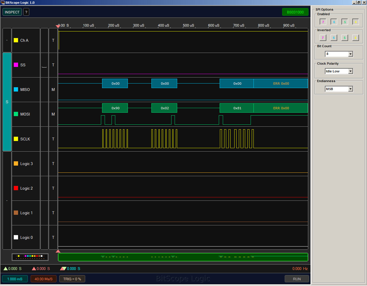
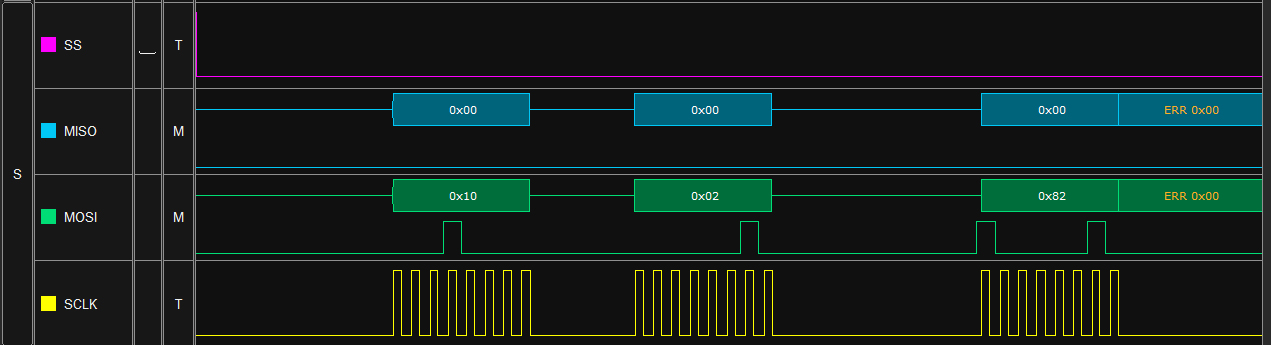
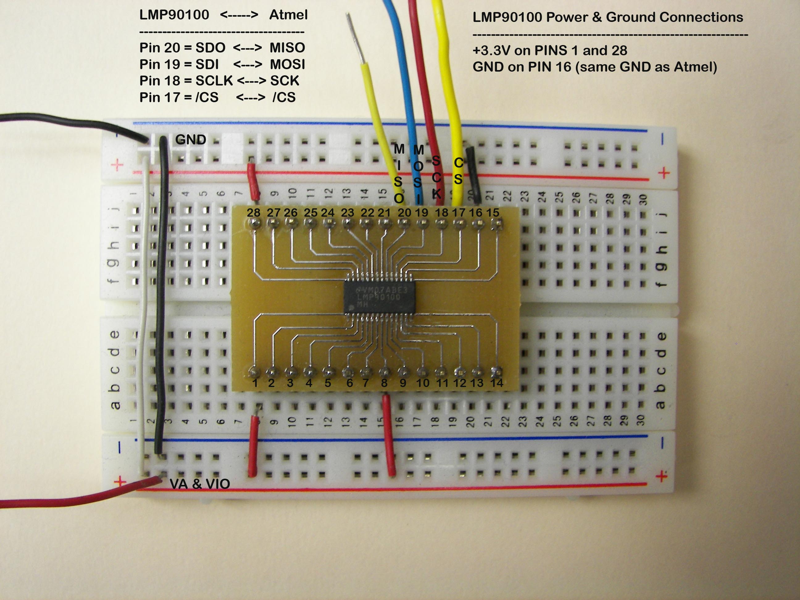
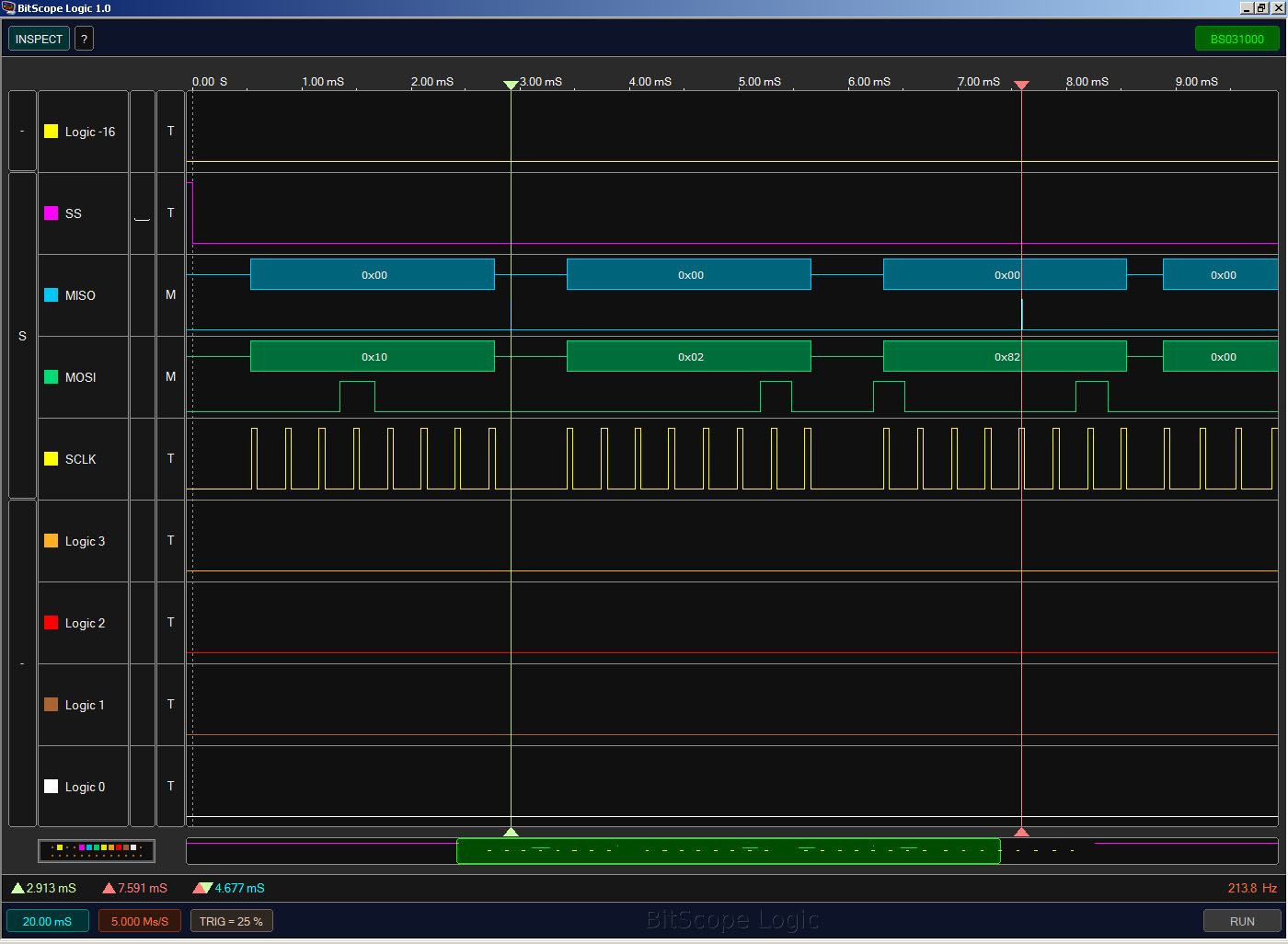
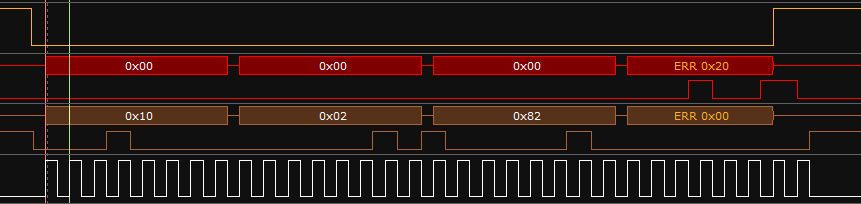
I am having problems with SPI communications.  I have initialized my SPI inteface with cpol=0, cpha=1, MSB first, and 4-wire mode. 

Attached is a jpg file showing CSB, SCLK, MOSI, and MISO when trying to read CH0_CONFIG Register 0x21.

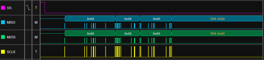
What am I doing wrong?

  • Hi Bradley,

    Your LA trace looks a little unusual - I'm not used to seeing the SCLK, MOSI and MISO all have what look to be the exact same set of data.  How are you connecting into the LMP90100?  Can you post us a schematic of your setup?

  • I did have a connection problem with my Microcontroller and LMP90100.  I have corrected that problem now and I am attempting to read CH0_CONFIG Register 0x21 from LMP90100 ADC and I should get the default value of 0x70, but I always get back zero.

    My LMPread function for register 0x21 sends Transaction-1 which is:  INSTR1, URA and then sends Transaction-2 which is INSTR2

        spiWrite(chr(INSTR1))                                            #sends 0x90
        spiWrite(chr(URA))                                                  #sends 0x02
        x = ord(spiXfer(chr(INSTR2)))                               #sends 0x81

    Attached is the updated LA trace.

    Is there something that I am missing because I only receive zero back when the default vaule for this register is suppose to be 0x70?  I have tried other registers whose default value is also non-zero with the same result of zero.

  • I am try to do a simple read and only receive back zero.  Do I need to write something before I can try a simple read?

  • Please take a look at the MSP430-LMP90100 interfacing application note and code zip for examples

    http://www.ti.com/lit/an/snaa134/snaa134.pdf 

    http://www.ti.com/litv/zip/snac029 <-- code zip

  • Hey.

    I have a similar problem. You gotta fix it?, You could tell me what you did?.

    Thank you.

  • I did have some problems with the SPI data I was trying to send to the ADC.  I now can send the correct SPI data, but still get no response from ADC.

    The logic analyzer attachment was created when I tried to follow the example on page 41 of the LMP90100 RevN Datasheet which is 17.4.2 Reading from Register Example.  That simple example would not even work correctly.

    address=34, 0x22
    INSTR1=16, 0x10
    URA=2, 0x02
    LRA=2, 0x02
    INSTR2=130, 0x82
    return value=0, 0x00

    I did not receive any support other than look at the example code which I already had done.  I think this ADC is a great product and I would love to get it working, but it took too long and no real support for it.  My solution was to use a different ADC (LTC2498).  If I can figure out what went wrong or get some support to find a solution, then I will post it here.

    Good luck, Javier!

  • Bradely/Javier,

    I attach here a scope shot for the register read transaction you mention above. The top waveform is CSB, then MISO, MOSI and CLK. If you look at the MOSI waveform, you can see first the instruction byte1 INSTR1 (0x10) is sent, followed by upper address byte URA (0x02) and instruction byte2 INSTR2 (0x82). Following this, we read the data byte on MISO (0x13) which is the default value for register 0x22. I used MSP430 USCIA1 (SPI mode) peripheral to control LMP90100. I also did a gpio bit bang version example (instead of using USCIA1 peripheral) and the scope shot is also attached below.

    Let me know if this helps. Please check if LMP90100 Evaluation Board is powered correctly. You need to provide two supplies (VA & VIO).

    Thanks,

    Vishy

  • I attach the scope shots below

  • Vishy Viswanathan said:

    I also did a gpio bit bang version example (instead of using USCIA1 peripheral) and the scope shot is also attached below.

    Let me know if this helps. Please check if LMP90100 Evaluation Board is powered correctly. You need to provide two supplies (VA & VIO).

    Thanks,

    Vishy

    Vishy,

    I was using an 8-bit Atmel AVR micro-controller and separate board that I made for the LMP90100 (attached is picture of the LMP90100 board). 

    I have tried using both the built-in SPI interface (hardware) and wrote a gpio bit bang version (software).  With either the hardware or software SPI, I do not receive a response from LMP90100 (trying the example on page 41 of the LMP90100 RevN Datasheet which is 17.4.2 Reading from Register Example). 

    The steps you outlined in your explanation of the oscilloscope attachments, specifically:

    1) instruction byte1 INSTR1 (0x10) is sent

    2) followed by upper address byte URA (0x02)

    3) instruction byte2 INSTR2 (0x82)

    4) we read the data byte on MISO which should be (0x13) the default value for register 0x22

    are exactly what I have tried doing using both methods the hardware and software SPI.  Could you provide the code you wrote for your gpio bit bang version?  I don't know if it will help, but maybe there is something simple that I am missing. 

    Thanks,

    Brad

  • Brad,

    I attach here a zip file with the bitbang code. The file TI_MSP430_spi_BITBANG.c has all the functions you need to look at. There’s a SPI setup function to setup bitbang pins. There’s also SPI read and write functions that calls bitbang_in and bitbang_out to read and write out data. Let me know if you have questions.

    Thanks,

    Vishy4670.bitbang.zip

  • Vishy,

    Since the bit-banged SPI software version is slower than the hardware SPI, I noticed on the logic analyzer capture the drdyb signal asserting about every 4.6ms. 

    Do I need to complete writing INST1, UAB, INST2 before the next assertion of drdyb, right? 

    Previously, I had not waited for drdyb to assert after asserting CS.  Using the hardware SPI, I have written INST1, UAB, INST2 before next drdyb, but I still get no response when trying to read from ADC. 

    What suggestions, if any, do you have for me to try?

    Thanks,

    Brad

  • Brad,

    drdyb matters when reading out of ADC_DOUT registers. There's no timing dependency for reading other registers with drdyb. Could you share with me your atmel bit bang code & also the schematic showing how the atmel MCU SPI (or GPIO) pins are setup?

    Thanks,

    Vishy

  • Vishy,

    Attached is Adobe PDF file with schematic and bit-bang code.   I am using an RF200 module from Synapse Wireless.  The microcontroller on the module is Atmel ATMega128RFA1. 

    I have also used the Synapse Wireless Forum (http://forums.synapse-wireless.com/showthread.php?t=2152&highlight=spi+communications+problems) to make sure I was using their version of Python to program the module correctly.  I have tried their built-in version of SPI and the attached code is my bit-bang implementation.  I think there must be something that I am missing when trying to read from the ADC.

    3034.TI Forum - Post.pdf

    Thanks,

    Brad

  • Brad,

    In your code, I see both the spiWriteReg and spiReadReg functions use SPI_MOSI line. Shouldn't the spiReadReg function use SPI_MISO line instead?

    >>> My bad: At the end I see you are using the MISO line.

    I am still reviewing. If I find something else, will let you know.

    thanks,

    Vishy


  • Please see below my inputs after reviewing your python code:

    a)      In lmpSetupSPI(), please include

    SetPinDir(SPI_MISO, False)                     #just to be sure pin is configured as GPIO input

    b)      In SPIReadReg and SPIWriteReg, please try with clock polarity low to high instead of high to low (as in the bit bang code)

            writePin(SPI_SCK, False)                  # Toggle the clock line ( low to high polarity)

            writePin(SPI_SCK, True)                   # Toggle the clock line

    c)       SPIWriteReg: How is this function used? Not particularly useful as it won’t work with a lmp register address. At the end of SPIWriteReg why there is \CS toggle?

  • Vishy,

    Thank you for your review of my code because with your suggestions and a few more changes, I can now read and also write to the LMP90100 registers.

    Your suggestion a) I had already done, but setting it up as a watched input caused problems.  I had the MISO pin setup like this:

        # Set MISO as a watched input
        setPinDir(SPI_MISO, False)                               # Set pin as input
        setPinPullup(SPI_MISO, True)                           # Enable internal pull-up    
        monitorPin(SPI_MISO, True)                              # Monitor for drdyb assertion

    Your suggestion b) almost correct but ending up needing to be high first and then low.

            writePin(SPI_SCK, True)                 # Set clock line high
            writePin(SPI_SCK, False)                # Set clock line low

    Your suggestion c) exactly correct because I didn't finish writing/testing that function since I needed to be able to read a register first before I could write.

    Attached is the bit-bang version with the changes so I can read and write to the registers in the LMP90100. 

    2043.TI Forum - code2.pdf

    Now I can move onto testing other parts of the ADC.

    Thank you,

    Brad

  • Hello Vishy,

    I face very similar problem that Brad faced: ATmega128RFA1 and LMP90100 integration, but I'm trying to achive my goal through USART in SPI mode, and ported your SPI read/write funtions from library above.

    #include <asf.h>
    #include <TI_LMP90100.h>
    #include <TI_LMP90100_register_settings.h>
    
    /* Calculation of UBBRR value. */
    #define FOSC 8000000 // Clock Speed
    #define BAUD 230400 // Desired bps
    #define MYUBRR (FOSC/2/BAUD-1)
    
    /* USART line definitions. */
    #define USARTDDR DDRD //!< The data direction register for the USART lines.
    #define XCKPIN PD5 //!< The bit position for the USART XCK line.
    
    /* ~SS line macros. */
    #define SSPIN PD4 //!< The pin used as ~SS to slave.
    #define SSDDR DDRD //!< The data direction register for the ~SS line.
    #define SSPORT PORTD //!< The port register for the ~SS line.
    #define SETSSDIR SSDDR |= (1<<SSPIN); //!< Set output direction for ~SS line.
    #define CLR_CSB SSPORT |= (1<<SSPIN); //!< Set ~SS line high.
    #define SET_CSB SSPORT &= ~(1<<SSPIN); //!< Set ~SS line low.
    
    /* RX pin setup */
    
    #define RXPIN PD2 // MISO pin
    #define RXDDR DDRD // data direction register for MISO pin
    #define RXPORT PORTD // port register for MISO pin
    #define RXDIR_SET RXDDR |= (0<<RXPIN)
    #define RX_SET RXPORT |= (1<<RXPIN)


    /* PWM init in phase corr mode */
    void init_oc3_pwm (void)
    {
    	ICR3=125;			//TOP
    	TCCR3A = 0b10101010; // Phase corr PWM 16 Bit,
    	TCCR3B = 0b00010001; // Used NO Prescaler, TOP=ICR3
    	TCNT3 = 0;           // Reset TCNT3
    
    	DDRE|=(1<<DDE5);
    }
    
    /*  Initialize on-chip USART0 in Master SPI Mode and set the
     *  required port directions. There are no other masters on the
     *  bus, so the XCK line is configured as output.
     *
     *  \param spimode  SPI mode. Must be 0, 1, 2 or 3.
     *  \param myubrr  SPI speed. Value to put into USART Baud Rate Register.
     *
     *  \note  SPI speed in bits per second: bps = CPUFREQ/(2*(brreg+1)).
     *  \note  brreg value: brreg = (CPUFREQ/(2*bps))-1.
     */
    void init_usart1_spi( unsigned char spimode, unsigned int myubrr )
    {
    	// Baud rate must be set to 0 prior to enabling the USART as SPI
    	// master, to ensure proper initialization of the XCK line.
    	UBRR1 = 0;
    	
    	// Set XCK line to output, ie. set USART in master mode.
    	USARTDDR |= (1<<XCKPIN);
    	
    	// Set USART to Master SPI mode.
    	UCSR1C = (1<<UMSEL11) | (1<<UMSEL10);
    	
    	// Set clock polarity and phase to correct SPI mode.
    	if( spimode & 0x01 ) UCSR1C |= (1<<UCPOL1);
    	if( spimode & 0x02 ) UCSR1C |= (1<<UCPHA1);
    	
    	// Enable RX and TX.
    	UCSR1B = (1<<RXEN1) | (1<<TXEN1);
    
    	
    	// Set baud rate. Must be set _after_ enabling the transmitter.
    	UBRR1 = myubrr;
    }
    
    //------------------------------------------------------------------------------
    //  void TI_LMP90100_SPIWriteReg(uint8_t addr, uint8_t value, uint8_t *pURA)
    //
    //  DESCRIPTION:
    //  Writes "value" to a single configuration register at address "addr". If
    //  "addr" lies within the same segment as "*pURA", it takes 1 less transaction
    //  to write the value.
    //------------------------------------------------------------------------------
    void TI_LMP90100_SPIWriteReg(uint8_t addr, uint8_t value, uint8_t *pURA)
    {
    	uint8_t new_URA, inst;
    	
    	new_URA = (addr & LMP90100_URA_MASK)>>4;			                           // extract upper register address
    
    	SET_CSB;										                               // /CS enable
    	
    	if (*pURA != new_URA)									                       // if new and previous URA not same, add transaction 1
    	{
    		inst = LMP90100_INSTRUCTION_BYTE1_WRITE;                                   // Transaction-1
    		
    		while ( !( UCSR1A & (1<<UDRE1)) );                                         // Wait for TXBUF ready
    		UDR1 = inst;												               // Send instruction
    		
    		while ( !( UCSR1A & (1<<UDRE1)) );                                         // Wait for TXBUF ready
    		UDR1 = new_URA;                                                            // Send upper register address
    		
    		*pURA = new_URA;                                                           // save new URA
    		
    	}
    	
    	inst = LMP90100_WRITE_BIT | LMP90100_SIZE_1B |(addr & LMP90100_LRA_MASK);    // lower register address
    	while ( !( UCSR1A & (1<<UDRE1)) );                                           // Wait for TXBUF ready
    	UDR1 = inst;                                                                 // Send lower register address
    	
    	while ( !( UCSR1A & (1<<UDRE1)) );                                           // Wait for TXBUF ready
    	UDR1 = value;                                                                // Send data value
    	
    	while ( !( UCSR1A & (1<<UDRE1)) );                                           // Wait for TXBUF ready
    	while ( !(UCSR1A & (1<<TXC1)) );											 // Wait for TX complete
    	
    	CLR_CSB;									                                 // /CS disable
    	
    }
    
    
    //------------------------------------------------------------------------------
    //  uint8_t TI_LMP90100_SPIReadReg(uint8_t addr, unit8_t *pURA)
    //
    //  DESCRIPTION:
    //  Reads a single configuration register at address "addr" and returns the
    //  value read. If "addr" lies within the same segment as "*pURA", it takes 1
    //  less transaction to read the value.
    //------------------------------------------------------------------------------
    uint8_t TI_LMP90100_SPIReadReg(uint8_t addr, uint8_t *pURA)
    {
    	uint8_t x, new_URA, inst;
    
    	new_URA = (addr & LMP90100_URA_MASK)>>4;                                     // extract upper register address
    	
    	SET_CSB;
    	RXDIR_SET;										                               // /CS enable
    	RX_SET;	
    	
    	if (*pURA != new_URA)									                       // if new and previous URA not same, add transaction 1
    	{
    		inst = LMP90100_INSTRUCTION_BYTE1_WRITE;                                   // Transaction-1
    		
    		while ( !( UCSR1A & (1<<UDRE1)) );                                         // Wait for TXBUF ready
    		UDR1 = inst;												               // Send instruction
    		
    		while ( !( UCSR1A & (1<<UDRE1)) );                                         // Wait for TXBUF ready
    		UDR1 = new_URA;                                                            // Send upper register address
    		
    		*pURA = new_URA;                                                           // save new URA
    		
    	}
    	
    	inst = LMP90100_READ_BIT | LMP90100_SIZE_1B | (addr & LMP90100_LRA_MASK);    // Transaction-2
    	
    	while ( !( UCSR1A & (1<<UDRE1)) );                                           // Wait for TXBUF ready
    	UDR1 = inst;                                                                 // Send lower register address
    
    	while ( !( UCSR1A & (1<<UDRE1)) );								             // Wait for TXBUF ready
    	UDR1 = 0x00;														         // Dummy write so we can read data
    			
    	while ( !( UCSR1A & (1<<UDRE1)) );								             // Wait for TXBUF ready
    	while ( !(UCSR1A & (1<<TXC1)) );											 // Wait for TX complete
    	x = UDR1;																	 // Read data
    	
    	CLR_CSB;									                                 // /CS disable
    
    	return x;
    }
    
    int main (void)
    {
    	uint8_t prev_URA;                                                            // Previous Upper Register Address (URA)
    	uint8_t count, i, addr, val;
    	
    	
    	board_init();
    	init_usart1_spi(2, MYUBRR);
    	prev_URA = LMP90100_URA_END;                                                 // Initialize prev_URA to invalid segment
    	
    	//init_oc3_pwm();
    	//OCR3C = 12;
    	TI_LMP90100_SPIWriteReg(TI_LMP90100_CH1_INPUTCN_REG, 0x12, &prev_URA);


    	while (true)
    	{
    		prev_URA = LMP90100_URA_END;
    		val = TI_LMP90100_SPIReadReg(TI_LMP90100_CH1_INPUTCN_REG, &prev_URA);
    		//delay_ms(100);
    		//TI_LMP90100_SPIWriteReg(TI_LMP90100_CH1_INPUTCN_REG, 0x12, &prev_URA);
    		delay_ms(100);
    		//val = TI_LMP90100_SPIReadReg(TI_LMP90100_RESETCN_REG, &prev_URA);
    		//delay_ms(100);
    	}
    	// Insert application code here, after the board has been initialized.
    }
    

    However, I was able to produce exactly the similar timing diagram as on your first scope image - except MISO answer from LMP90100 :((((

    After checked galvanic connection from pin-to-pin, now in doubt, if the IC was damaged during I soldered the protoboard?!

    Any other suggestions?

    Thank you, and best regards, 

    András Kovács

  • Andr��s Kov��cs said:

    After checked galvanic connection from pin-to-pin, now in doubt, if the IC was damaged during I soldered the protoboard?!

    Any other suggestions?

    András Kovács,

    After I was able to communicate with the LMP90100,  I wrote an error check routine that I use to test newly constructed boards. 

    My simple error check routine is the following:

        // Runs periodically and sets an error flag if I can not communicate with the LMP90100
        regValue = lmpRead(0x22)                    // LMP90100 Register with non-zero value
        if  regValue != 0x13:                                  // Error check - Read result from a ADC register with non-zero value
            flagError1 = 1                                        // Set error flag


    This may help you to isolate your problem.

    Brad

  • Thanks, Brad,

    for your proposal. Finally it was a mistake: MISO/MOSI cables twisted...

    Now I struggle with SS line.  While I write in the code: 

    while ( !( UCSR1A & (1<<RXC1)) );   // Wait for data to be received
    CLR_CSB;                            // CS disable

    it deasserts two bits earliear than needed :-o

    ???

  • Bradley:

    I hope you got this working by now.

    I was browsing old messages and see you fell into the same trap I did.  That is that the data sheet instructions for this part are mostly crap.

    You are sending a 0x90 as the first byte. The data sheet should say that you ALWAYS send a 0x10 to do WRITE of the register..  I have no idea why the English challenged author of the data sheet included any reference to 0x90.  You NEVER want to read the address register.  You want to hold a local copy of the register address and ALWAYS write the register stuff from local memory.  I have no idea why the National guys even put in a function to read the address.

    I see that someone at TI finally told you to write 0x10 as the first byte rather than 0x90.