This thread has been locked.

If you have a related question, please click the "Ask a related question" button in the top right corner. The newly created question will be automatically linked to this question.

INA818: Common Mode range

Part Number: INA818
Other Parts Discussed in Thread: INA828,

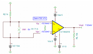
I've downloaded the Common-Mode Input Range Calculator for Instrumentation Amplifiers but it does not include INA818. Is there any model that would be identical in this tool to represent the INA818? I see the INA828 available for example. In my design I use a +5/-5V supply, Gain=700, and a VREF=-2.9V. I am trying to verify the maximum input amplitude and common mode range. My test board shows unexpected issues with a VDIFF=5mV and VCM=7.5mV. Much thanks. Falk 

  • Hi Falk,

    I put a circuit together per your design requirements. With Gain of 700V/V, output will swing at +/-1.76Vpp. 

     INA818 E2E-1 06012021.TSC

    This is your Vcm mode range vs. Vout with Vref = 0. 

    This is the INA818's transfer function. 

    If you have additional questions, please let me know. 

    Best,

    Raymond

  • Thank you Raymond. My reference voltage is negative; it is -2.9V, not +2.9V. I've updated the TINA circuit and ran it with 5mV differential input swing (e.g. VI-=5mV, VI+=10mV). The simulation predicts: Vout=610mV (same as the data sheet formula), V(Rg-)=-13mV, and V(Rg+)=-8mV

    My hardware also measures ~610mV on the output , but the voltage on the gain resistor measure much different: V(Rg-)=-532mV and V(Rg+)=-527mV

    In my design it is important to know the voltage range for the gain resistor pins as we use a mux there to switch between different resistors. Based on Fig 55 of the INA818 datasheet I had expected the voltage on the resistor to be identical to the voltage on the positive and negative input terminal. However, it seems in practice that is not true. Can I assume that the difference is due to the forward voltage drop across the super-beta NPN as shown in the Functional Block diagram (8.2)?  Why does the TINA Spice model not include this offset voltage in the model? Would the HSPICE model react any different ? 

    Much thanks, Falk

  • Hi Falk,

    Here is my simulation with Vref = -2.9Vdc, which is in agreement with yours. 

    In your bench setup, the voltage delta across Rg gain resistor is 5mV, which is the same as the simulation. My guess is your measurement may be affected by the DMM used in the measurement. If you use high impedance DMM, you may get a close value as the simulation. At least the current go through Rg gain resistor is in agreement in both cases. 

    Q: Why does the TINA Spice model not include this offset voltage in the model? Would the HSPICE model react any different ? 

    We have Vos modeled in the simulation, a typical Vos is 10uV, with Gain=700V/V, Vos measured at output should be approx. 7mV, see the simulation. I reset Vref = 0, so it is easier to observe the Vos, otherwise, it will be (-2.9V - 7.03mV).

    We do not use HSpice model. 

    If you have additional questions, please let us know. 

    Best,

    Raymond

  • Hi Raymond, 

    I am not worried about VOS - the output voltage on the bench looks correct. My concern is purely the actual pin voltage at the gain resistor. I don't think the DMM affects the measurement. We use a high-end Fluke with a very high input resistance well into the mega-ohms, and secondly I just re-checked the voltage measured directly between VIN+ and RG and VIN- and RG, and there is about a 500mV offset. Based on your simulation it shouldn't be more than ~20mV. As I measure between VIN and RG the DMM shouldn't have any negative impact since these voltage should be nearly identical. I don't see how the DMM could shift the RG pin to -500mV. I have two boards and they both respond identically. Best regards, Falk

  • Hi Falk, 

    Can I assume that the difference is due to the forward voltage drop across the super-beta NPN as shown in the Functional Block diagram (8.2)?

    Yes, you are correct. There is a Vbe diode level shift between +IN and -IN inputs and RG gain resistor, which is NOT reflected in INA818 model.  RG voltage level, however, for all practical purposes is an internal node that does not affect inner-working of the INA818 macro-model but makes creating model more straight forward.

    Best,

    Raymond

  • That works for me. I assume the magnitude of that Vbe diode shift will be fairly stable near the measured 500mV, and probably not exceed much more than 700mV over temperature. Thankyou for all your responses!