This thread has been locked.

If you have a related question, please click the "Ask a related question" button in the top right corner. The newly created question will be automatically linked to this question.

PGA308: OTP memory does not program

Part Number: PGA308

Good day, 

I am running into a problem with PGA308 when programming OTP memory. All OTP registers return 0xFF. The system is powered off of 5V power supply the entire time.

Here are my calibration steps: 

1) Run calibration loop in Software Lock mode - no problem. Here is the function that I am implemented for that: 


    void calRunInRam(int8_t coarse_offset)
    {
        uint16_t cfg0 = 0x0000;
        cfg0 = cfg0 | PGA308_OUTPUT_GAIN__2 << 13; //Output gain in the D[15:13]
        cfg0 = cfg0 | (0 << 12); // Input mux in D12
        cfg0 = cfg0 | PGA308_INPUT_GAIN__200 << 8; // Input gain in D[11:8]
        if (coarse_offset < 0){
            cfg0 = cfg0 | 0x80 | abs(coarse_offset); // Offset in D[7:0]
        } else {
            cfg0 = cfg0 | abs(coarse_offset); // Offset in D[7:0]
        }

        bankValues[PGA308_REG__ZDAC] = 0x0000;
        bankValues[PGA308_REG__GDAC] = 0x4000;
        bankValues[PGA308_REG__CFG0] = cfg0;
        bankValues[PGA308_REG__CFG1] = 0x1780;
        //bankValues[PGA308_REG__CFG2] = 0x0C00; // for 5V system
        bankValues[PGA308_REG__CFG2] = 0x0800; // for 3V system
        bankValues[PGA308_REG__CHKS] = calculateChecksum(bankValues, 5);
        
        // Enter Software Lock Mode
        writeRAMReg(PGA308_REG__SFTC, PGA308_SFTC__SWL_SOFTLOCK);

        // Write stored registers
        writeRAMReg(PGA308_REG__ZDAC, bankValues[PGA308_REG__ZDAC]);
        writeRAMReg(PGA308_REG__GDAC, bankValues[PGA308_REG__GDAC]);
        writeRAMReg(PGA308_REG__CFG0, bankValues[PGA308_REG__CFG0]);
        writeRAMReg(PGA308_REG__CFG1, bankValues[PGA308_REG__CFG1]);
        writeRAMReg(PGA308_REG__CFG2, bankValues[PGA308_REG__CFG2]);
        writeRAMReg(PGA308_REG__CHKS, bankValues[PGA308_REG__CHKS]);
    }

2) Loop also polls the PGA over I2C, and as soon as we hit the mid-range readout, I want to write calibration values into OTP.

3) Writing in to OTP looks as following:

    void calSaveIntoOTPMem(int8_t coarse_offset)
    {
        // Enter standalone mode
        
        writeRAMReg(PGA308_REG__SFTC, 0x0000);
        writeRAMReg(PGA308_REG__OTPS, 0x8000); // OTP EN
        readRAMReg(PGA308_REG__OTPS);

        //lets write all the registers first

        writeOTPReg(PGA308_BANK__U1, PGA308_REG__ZDAC, bankValues[PGA308_REG__ZDAC]);
        writeOTPReg(PGA308_BANK__U1, PGA308_REG__GDAC, bankValues[PGA308_REG__GDAC]);
        writeOTPReg(PGA308_BANK__U1, PGA308_REG__CFG0, bankValues[PGA308_REG__CFG0]);
        writeOTPReg(PGA308_BANK__U1, PGA308_REG__CFG1, bankValues[PGA308_REG__CFG1]);
        writeOTPReg(PGA308_BANK__U1, PGA308_REG__CFG2, bankValues[PGA308_REG__CFG2]);
        writeOTPReg(PGA308_BANK__U1, PGA308_REG__CHKS, bankValues[PGA308_REG__CHKS]);

        writeOTPReg(PGA308_BANK__FTEST, PGA308_OTP_REG_BSEL1, 0x0001);
            
        writeRAMReg(PGA308_REG__OTPS, 0x0000); // OTP EN
        writeRAMReg(PGA308_REG__SFTC, 0x0000);
        delay(3);
        
        //lets confirm all the registers by reading them
        readRAMReg(PGA308_REG__SFTC);
        readRAMReg(PGA308_REG__OTPS);
        readOTPReg(PGA308_BANK__FTEST, PGA308_OTP_REG_BSEL3);
        readOTPReg(PGA308_BANK__U3, PGA308_REG__ZDAC);
        readOTPReg(PGA308_BANK__U3, PGA308_REG__GDAC);
        readOTPReg(PGA308_BANK__U3, PGA308_REG__CFG0);
        readOTPReg(PGA308_BANK__U3, PGA308_REG__CFG1);
        readOTPReg(PGA308_BANK__U3, PGA308_REG__CFG2);
        readOTPReg(PGA308_BANK__U3, PGA308_REG__CHKS);
    }

Here is the implementation of writeOTPReg:

    void kickOneWire()
    {
        Serial1.write(PGA308_SYNC);
        Serial1.flush();
    }

    void writeRAMReg(uint8_t ptr, uint16_t value)
    {
        kickOneWire();
        uint8_t buf[3];

        buf[0] = PGA308_ACCESS_RAM | PGA308_ACCESS_WRITE | ptr;
        buf[1] = value & 0xFF;
        buf[2] = value >> 8;
        
        Serial1.write(buf,3);
        Serial1.flush();
    }

    void writeOTPReg(uint8_t bank_ptr, uint8_t reg_ptr, uint16_t value)
    {
        kickOneWire();

        uint8_t buf[4];

        // Transfer sync, addr and data
        buf[0] = PGA308_ACCESS_OTP | PGA308_ACCESS_WRITE | (bank_ptr << 3) | reg_ptr;
        buf[1] = value & 0xFF;
        buf[2] = value >> 8;
        
        Serial1.write(buf,3);
        Serial1.flush();
                readRAMReg(PGA308_REG__OTPS);
        delay(4); //mandatory 3ms delay white OTP is being written
                readRAMReg(PGA308_REG__OTPS);
    }

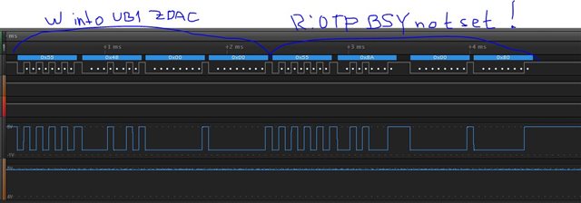
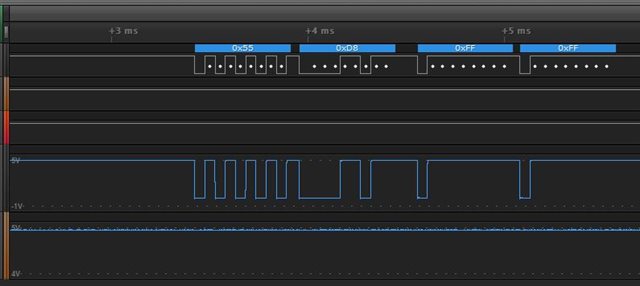
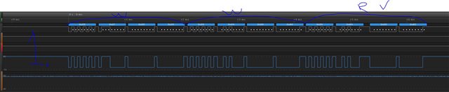
What I observe is that the OTP BSY bit never sets, and when I read OTP back all I get is 0xFF. I have confirmed with the logic analyzer that I am not writing 0xFFs at all.

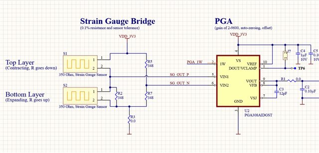
What am I doing wrong? I also attached schematics snippet for your reference. Thanks!

  • Hi Dmitrii,

    I'm looking into this but I have a couple of basic starter questions regarding your setup, as I don't want to make any assumptions.

    1. Just to confirm, you are using a 5V supply when programming the device, rather than the 3.3V shown in the schematic? The OTP will fail to program if the device supply is below ~4.5V.
    2. Are you using the PGA308EVM to do your programming, or an external terminal/different software and hardware?
    3. Is there a pullup resistor on the 1W line that is not shown in the schematic, and if so what is its value?
    4. Are you testing on a fresh PGA308 device that has never undergone OTP?

    And some more questions.

    5. Have you been able to confirm that the proper checksum is being calculated for the CHKS register?
    6. Have you been able to successfully read back the RAM registers after you write to them in software lock mode, to verify they are being written correctly?
    7. Have you been able to confirm that the device is successfully exiting the software lock mode? Does the OTP EN bit indeed get set high?

    Cheers,

    Jon

  • Hi JMac, 

    Thanks for the follow up questions. Here are the answers: 

    1. Yes, using ~4.98V at the VS and VREF, VClamp, and for bridge biasing, as opposed to the VDD_3V3 indicated on the schematics.

    2,3. I am using 5V Arduino compatible board, with two PFETs forming non-inverting open-drain output, with the pullup value of 4.7k.

    4. Yes, I have tested on two boards, one of which has never been programmed. Both show similar behavior, I don't really want to potentially brick more boards until there is a good reason to do so. I've tried programming different user banks and the same behavior persists. 

    5. Checked my checksum implementation with the user guide's values - look correct. But I suppose the problem happens earlier, as the registers seem to never get written with correct values.

    6. Yes, reading RAM registers works perfectly. 

    7. OTP EN bit indeed is high when I am trying to program the OTP.  I am including the logic analyzer traces for you to take a look as well. The problem that I am observing is that OTP BSY never gets set. Analog waveform is at the bottom for you to check the waveform and the voltage levels. 

  • Hi Dmitrii,

    Thank you for confirming your setup details and for sharing the waveforms. The circuit configuration appears to be correct from a hardware perspective.

    Would it be possible for you to try running the OTP script while still in Software Lock Mode? That is to say, instead of entering Standalone mode before writing the OTP memory (line 5 in the calSaveIntoOTPMem script), wait to enter the Standalone mode until after the write has completed (as you do on line 21 of that script).

    Cheers,

    Jon

  • Hi Dmitrii,

    Were you able to successfully program the OTP registers while in software lock mode? There is a note in the source code of the EVM that hints that the user may need to be in this mode in order to successfully execute the OTP write sequence, although it is not especially clear. If this did not solve the issue, please let me know and I can look into alternate solutions.

    Cheers,

    Jon