This thread has been locked.

If you have a related question, please click the "Ask a related question" button in the top right corner. The newly created question will be automatically linked to this question.

OPA375: input offset voltage

Part Number: OPA375

Hi, 

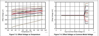
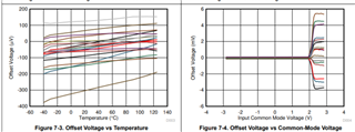
I was looking at the OPA375 and saw that this device has a max offset voltage of +-500uV under he test conditions. I then took a look at the figures lower in the datasheet and had a hard time understanding figure 7-4 (offset voltage vs common-mode voltage. I watched some of the precision labs videos but didn't quite find the answer to help explain why in figure 7-4 the offset voltage is off by an order of magnitude (5000uV@ CM of 2.5V) from the spec in the electrical characteristic table earlier on. Can you help me understand why this is different?

Thanks

  • The input offset voltage spec is always with the input CM mid-supply, figure 7-4 is just letting you know the input stage is starting to go non-linear within 5.5V-2.1 or within 3.4V of the positive supplies - many parts have this kind of effect, but this one is pretty extreme - maybe because of the low noise design. If you want better offset over higher input range, look for a zero crossover RRIO device. 

    I couldn't help notice the marque plot on the front page shows a common spot noise plot error. That rolloff at higher F most likely is the fact the device was in a very high gain setting to measure the noise, possibly rolling off the measured noise not because the input noise is rolling off, but amplifier gain is rolling off - maybe?

  • Hello User,

    The OPA375 is not a rail to rail input device, not RRI.

    Above [V+] - 1.2V, expect only a 'safety net' that protects against phase reversal by an input stage that crudely cover ups to V+ (when the main input transistors cut off due to lack of headroom.

    Micheal,

    I agree that front page drop off likely was due to op amp being set to 40dB and assuming 40dB actually occurred.

  • I was misinterpeting this plot the other day, the x-axis suggests it is for a +/-2.75V supply so that breakpoint is actually within 0.75V of the positive supply, which much more typical. This shift only becomes an issue for say unity gain buffer apps. If you need to get to the supply, again use a zero crossover RRI device