This thread has been locked.

If you have a related question, please click the "Ask a related question" button in the top right corner. The newly created question will be automatically linked to this question.

XTR111: RTI Noise

Part Number: XTR111
Other Parts Discussed in Thread: XTR300,

Hi,

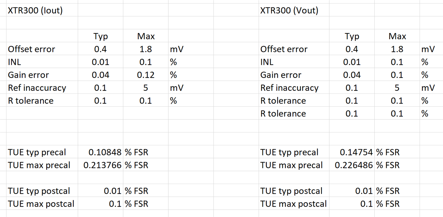
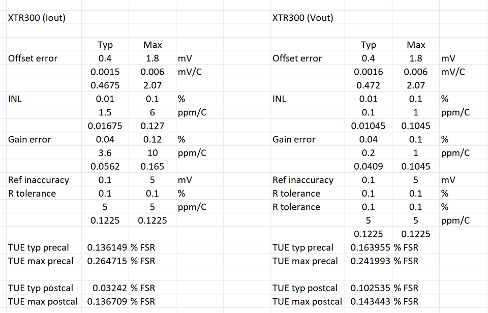
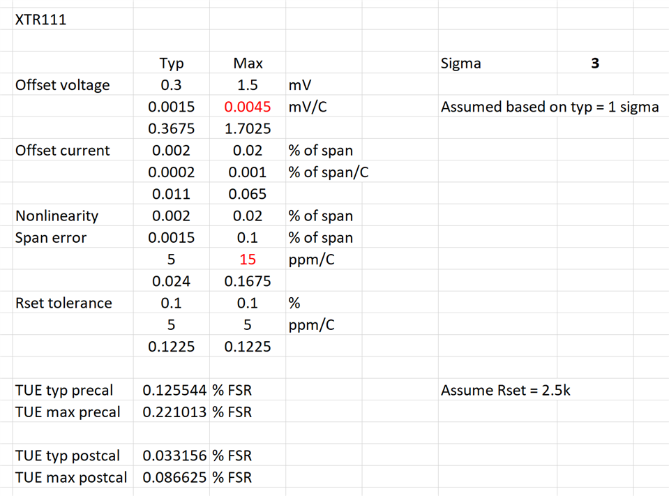
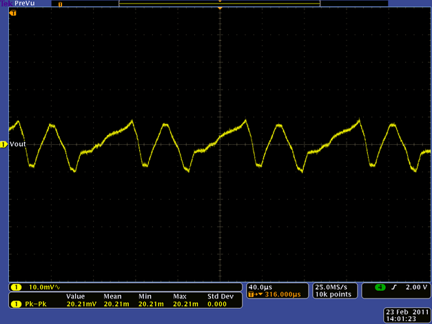
Can you please help me to relate the Figure 5(0.1Hz to 10Hz NOISE, RTI) to Figure 39 (Output Noise without Filter into 500Ω) in the datasheet (SBOS375C –NOVEMBER 2006–REVISED JUNE 2011) if Rset = 2k in terms of the peak amplitude

Best Regards,

Kavindu

  • Hi Kavindu,

    For Rset = 2k, the relationship from Iout/Vin is 5mA/V. Thus, an approximately +/-1.25uV noise pulse at the input as shown in Figure 5 would result in a +/-6.25nA output pulse at the output, which for a 500 ohm load is +/-3.125uV. This RTI noise is an approximation of what sort of noise would be required at the input of an ideal noiseless circuit, to cause an output noise equivalent to the actual performance of the real circuit.

    What Figure 39 is describing is the actual output glitch behavior, caused by the internal chopping of the current sources in the current mirror stage. +/-50mV on a 500 ohm load would be +/-100uA of peak glitch current. However, it is my understanding that over the entire cycle, the output noise averages out to the sort of specified noise values you would infer from the RTI plot. So you can think of Figure 5 as referring to the typical noise of the circuit when looked at over a longer time period, whereas Figure 39 shows the actual peaks of the output noise you will see over the 100us cycle if you checked with an oscilloscope.

    It is possible to attenuate the output noise by adding another filtering capacitor at the drain of the FET, as discussed in this document, if you are concerned the output noise will be too high for your application. Of course, keep in mind that more filtering capacitance means more rise time.

    Cheers,

    Jon

  • Hi Jon,

    Thanks for the clarification. I'm working on a precision transducer with an error budget of 0.1%, So this seems not the best fit. Can you suggest any other device from your portfolio that I can use

    Thanks,

    Kavindu 

  • Hi Kavindu,

    Another way to think about it is that the RTI noise represents a random, presumably Gaussian noise distribution that is characteristic of the part nonideality; while the output noise is more repeatable, with the chopping causing spikes in the positive and negative direction that are matched enough to cancel out when looked at over the entire 100us cycle. The minor deviations from this otherwise predictable behavior are reflected in the RTI noise.

    It is possible to attenuate these output spikes with an extra cap, as I mentioned. +/-0.1% of a 20mA signal is +/-20uA, or +/-10mV (or 20mVpp) on a 500 ohm load. To get the spikes down this low, you'd need a decently large cap, probably about 60-100nF, which would probably result in a rise time that is in the 80-120us range (see the document I linked in my last post for examples). Please comment on whether you think this would work or not. When you sample the load voltage with an ADC, is it a SAR or delta-sigma? You might also be able to do some oversampling or averaging on that side, since again the output noise from the mirror should appear to be pretty much zero-mean over a long interval.

    Can you share some more information about your application requirements? IE loop supply voltage, rise/response time, loading, etc. Is the operating environment at a fairly constant temperature or does it shift over a range?  Could you also consider an architecture that uses a two-wire transmitter instead?

    There are a few other devices that might be good options, but keep in mind that this current mirror architecture is pretty standard for TI's three-wire transmitters so you could see similar issues. For example, the XTR300 should be able to achieve about 0.01% typical FSR error after calibration, or 0.1% max, but this assumes an operating environment that is thermally stable enough that the drift over temperature can be ignored. Remember too that this is just the XTR300 itself and doesn't take other circuitry into account, which would also contribute error in a root-sum-of-squares fashion.

    However, the XTR300 also exhibits some output glitching, although I do not have any scope shots of it. From the "INTERNAL CURRENT SOURCES, SWITCHING NOISE, AND SETTLING TIME" section of the datasheet,

    "The accuracy of the current output mode and the dc performance of the IA rely on dynamically-matched current mirrors. Identical current sources are rotated to average out mismatch errors. It can take several clock cycles of the internal 100kHz oscillator (or a submultiple of that frequency) to reach full accuracy. This may dominate the settling time to the 0.1% accuracy level and can be as much as 100μs in current output mode or 40μs in voltage output mode. A small portion of the switching glitches appear at the DRV output, and also at the IMON and IAMON outputs. The standard circuit configuration, with RC, C4 , and CC, which are required for loop compensation and output protection, also helps reduce the noise to negligible levels at the signal output. If necessary, the monitor outputs can be filtered with a shunt capacitor."

    So even if you explore different options, you may find that you'll still need to use some output filtering to avoid noise pulses.

    Cheers,

    Jon

    Edit - adjusted recommended cap value, as +/-10mV is 20mVpp

  • Hi Jon,

    Thanks for the info.

    As you request, the transducer that I'm working with is Analog 3-wire load cell which is supposed to operate in the range of -20C to +70C, The response time can be in the vicinity of 1 ms. The supply voltage is 12 -24 V.

    Use of a filter cap should improve the noise performance as you suggest. in case this high frequency noise will not show up on a general digital voltmeter or a PLC?

    Another doubt I'm having is - is this noisy behavior existing only during the settling time to a step input? Or just prevalent all the time?

    Sorry for a lot of questions, just trying to learn as much as possible before I can use this.


    Best Regards,

    Kavindu

  • Hi Kavindu,

    Meeting the 0.1% error budget with those temperature requirements will be a little difficult. The XTR300 would actually struggle to meet the spec once the errors due to drift are considered (the typ error after cal is within the envelope, but the max error is not).

    If a precise low-drift resistor is used for Rset (5ppm or better), the XTR111 is better suited for the task. We don't specify a maximum drift, but if we assume the typical value represents 1 standard deviation, we can use 3*sigma for the max value and this will cover 99.7% of cases. Post-cal, you'd be looking at 0.087% maximum FSR error. If you want to go even more conservative and use 4 sigma, then the max error is unfortunately 0.105% FSR (it's worth noting that because the drift can be positive or negative, in reality the odds of the error budget being met are quite good - the typical FSR error will be 0.033%). You'd probably want to do your own final testing over temp to bin out outlier high-drift units, or look into doing a multi-point calibration. 

    I've attached the workbook I used to calculate the error, you can change the "sigma" value in the top right to adjust the calculations.

    xtr111 error budget.xlsx

    If you employ a filtering cap, the noise will still be visible at the output if viewed using an oscilloscope. I can't comment on whether or not it would be visible on a digital voltmeter or PLC without knowing more specifics, but again the actual noise you would see for different filter values is visible in the scope shots in that presentation I had linked earlier. Here it is again for reference - click here. Here's the scope shot for a 50nF cap. As you can see it's fairly high frequency, the pulses will look something like a 20-30kHz noise signal. Increasing the cap will decrease the peak-to-peak magnitude of the noise.

    Unfortunately this noise is always present on the output, not just immediately after a step of the input, because the current mirror is always switching. However, if a response time as high as 1ms is acceptable, then you should be able to severely attenuate this noise down to well below 20mVpp into the single digit mVpp range.

    Cheers,

    Jon