This thread has been locked.

If you have a related question, please click the "Ask a related question" button in the top right corner. The newly created question will be automatically linked to this question.

INA105: Could you help to check the DMM design?(Related PN: INA105KU ,OPA180ID,INA597IDT,INA121)

Part Number: INA105
Other Parts Discussed in Thread: OPA180, INA597

Hi Ti

Could you help to check the DMM design for us?

DMM SCH

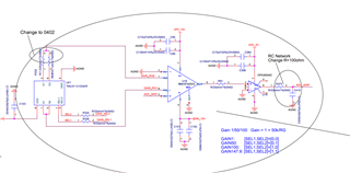
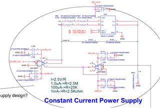
1.Constant Current Power design:U22 INA105KU+ U26 OPA180ID

MCU control Switch and change output current,Could you help to check the design?

I=1uA ~10mA.

Mark Question 1 in the attachment(Q1).

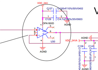
2. Buffer:U30 OPA180ID 

Just use it as a buffer.

Mark Question 2 in attachment.(Q2).

3. Differential Amplifier U53 INA597IDT Setting

5 Case:

Case1: 10 V Input,+10V to Pin3("+"),Pin2("-") connect to GND  ,V+=+10V, V- = -10V,So ouput is +5V

Case2: 10 V Input,+10V to Pin3("+"),Pin2("-") connect to GND  ,V+=+10V, V- =GND,So ouput is +5V

Case3: -10 V Input,-10V to Pin2("-"),Pin2("+") connect to GND  ,V+=GND, V- = -10V,So ouput is +5V

Case5: +/-10 V Differential Voltage ,+10V to Pin3("+"), -10V to Pin2("-")  V+=+10V, V- =-10V,So ouput is +10V

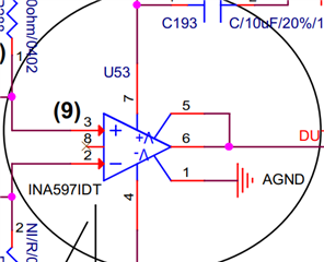
Mark Question 3 in attachment.(Q3).

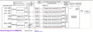
4. ADC GAIN Design: U18 INA121U +U19 OPA365AID

Mark Question 4 in attachment.(Q4).

  • Sorry, Correct:

    3 Case Only:

    Case1: 10 V Input,+10V to Pin3("+"),Pin2("-") connect to GND  ,V+=+10V, V- = -10V,So ouput is +5V

    Case2: -10 V Input,-10V to Pin2("-"),Pin2("+") connect to GND  ,V+=+10, V- = -10V,So ouput is +5V

    Case3: +/-10 V Differential Voltage ,+10V to Pin3("+"), -10V to Pin2("-")  V+=+10V, V- =-10V,So ouput is +10V

  • Hi,

    Thanks for your post. I can help you. In order to fully understand the schematic and get the full picture of how the amplifiers are implemented, more information on the inputs/outputs of each INA and OPA is needed. For instance, what is the input for the OPA180 in the buffer configuration in image 3? We need to know these voltage levels so that we can make sure you are not violating the input and output of the amplifier.  


    It also seems as if the images posted have the questions you intended to ask cutoff. One thing that would result in headroom issues is the very large 1Mohm resistive load in your current supply schematic if that is the intended load for the circuit. When convenient, could you please give more information on the schematic as mentioned above so we can further assist you with your schematic?

    -Ignacio

  • Hi Ignacio

    1.more information on the inputs/outputs of each INA and OPA is needed.

    >>>I Remak the input Voltage in this schematics, Could you help to check?

    2.One thing that would result in headroom issues is the very large 1Mohm resistive load in your current supply schematic if that is the intended load for the circuit

    Yes, It is the intended load, Then I can control the total load  less than 1Mohm, Limit the voltage incurrent= 1uA output

    For example:

    DUT_load is 10ohm, setting I=1mA. Input Voltage for OPA180 (U30)=10*1mA=10mV

    DUT_load is 100Mohm,  setting I=1uA. Input Voltage for OPA180=1uA*1Mohm=1V

    I think we can change 1Mohm to 4.7Mohm too. The limit voltage will up to 4.7V.

    What is your suggestion?

    Qin

  • Hi Ignacio

    Could you help to check the design?

    Or U need more information?

    Qin

  • Hi Qin,


    Sorry for the late response but I have reviewed the schematic you sent with the original questions and have the following feedback below.


    The question regarding the current source, it is a good current source design that provides plenty of flexibility however with this type of design a major issue is headroom constraints caused by the load and current intended to run. As long as you monitor the voltage at the load and make sure you don’t violate the input common voltage range of the OPA180, your current source is fine. In your specific design the input of the OPA180 (U26) must be within its specified input voltage range which can be found in the datasheet of the OPA180 under Electrical Characteristics in the Input Voltage Range section.


    Regarding your second question and the OPA180 configured in a buffer, any amplifier can be used as a buffer. With any amplifier, including those in buffer configurations, keeping track of the input common mode voltage range and output swing given the power supplies of the amplifier is a must. For the OPA180 in the buffer configuration with V+ of 24V and V- of 0V, your input common mode range must be within 0V < Vcm < 22.5. Similarly, the output swing of the OPA180 can be found, which depends on the load of the buffer and can be found in the datasheet up electrical characteristics. Remaining within the specified ranges of the OPA180 is critical for the part to function linearly. More information on these two concepts can be found in the TIPL video linked here:

    TI Precision Labs - Op Amps: Input and Output Limitations - Common mode voltage | TI.com Video

    TI Precision Labs - Op Amps: Input and Output Limitations - Output swing | TI.com Video


    I do have a question regarding the 0ohm resistors placed at the inputs of the INA597, could you tell me the intention with grounding these inputs?


    -Ignacio

  • Hi Ignacio

    Thank you for your great help.

    You Question:

    I do have a question regarding the 0ohm resistors placed at the inputs of the INA597, could you tell me the intention with grounding these inputs

    Qin=>

    Just for NI U53 if all input >0, Then we can useU46 and U98 for the test only.

    Backup for debugging, We will remove it in the final design.


    Qin