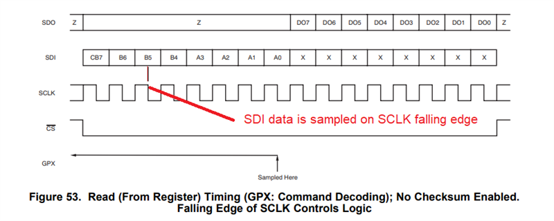
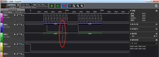
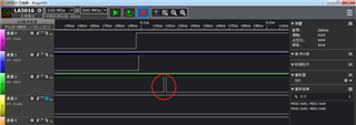
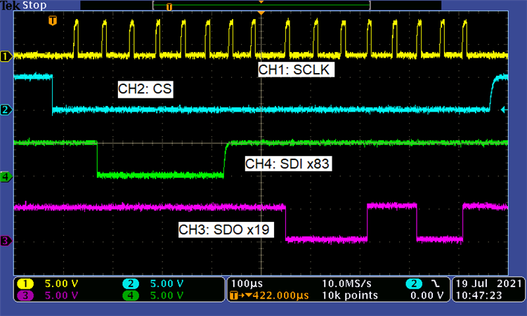
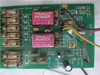
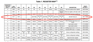
When debugging the PGA280, we sent the hex instruction 8300 to the PGA280 register 3 "set BUF time-out" (as shown in the figure). It should have got a return value of 19, but we did not receive any value, and the PGA280 did not respond.We suspect the chip didn't work because of the power supply.
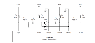
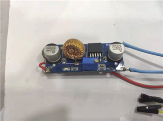
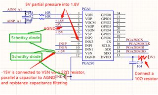
This is a typical power wiring diagram from the official documentation
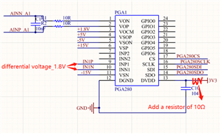
This is a typical power wiring diagram from the official documentation