Other Parts Discussed in Thread: LMV722,
Hello Expert,
I need your help and quick response after review about below.
Because our customer's production line has stopped.
Their product is running for more 7years.
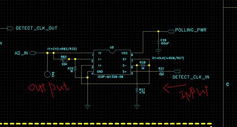
1. Here is schematic.
Could you please review and give me comment if there is fault and some issue?
VCC = 3V
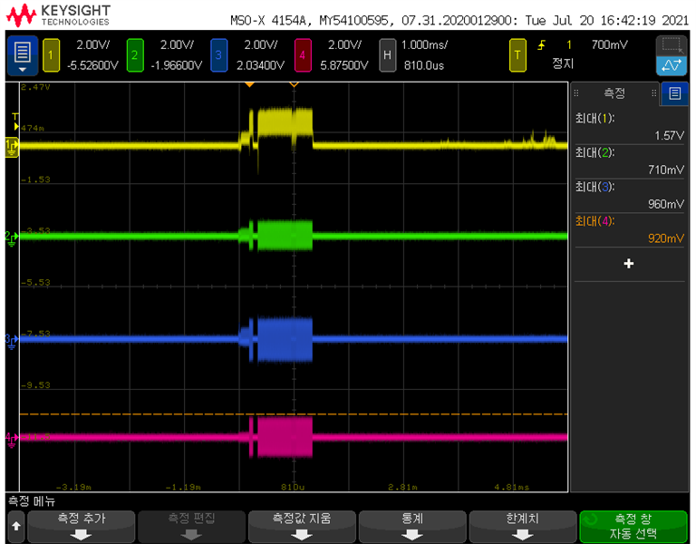
2. Waveform
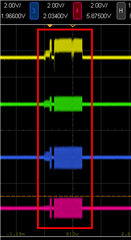
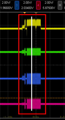
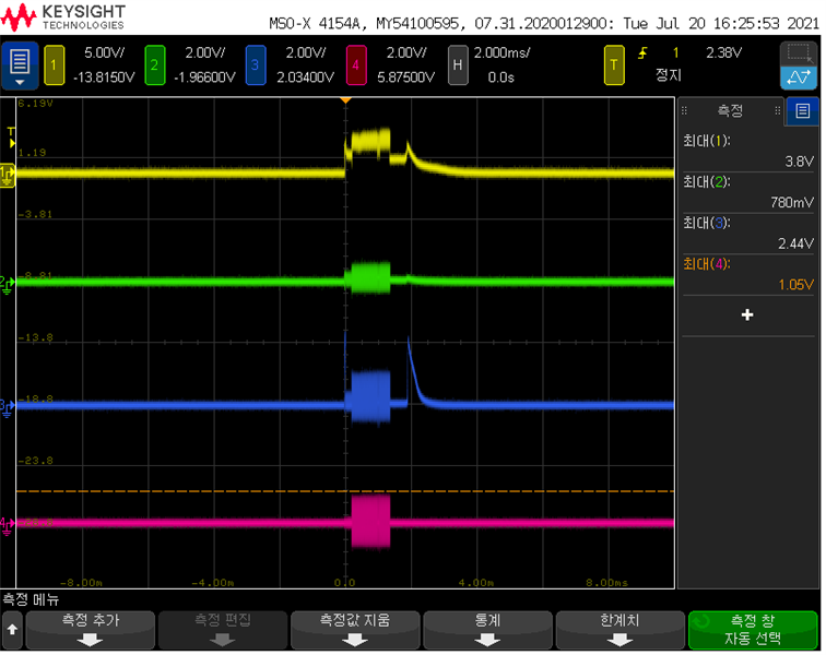
[CH1 : Pin1 // CH2 : Pin2 // CH3 : Pin3 // CH4 : Pin5]
DETECT_CLK_IN is clock signal which is generated from MCU for detecting RFID Signal.
Measured is max. voltage which is the right value of waveform image.
1) Good part (Date code : earlier than 2042)
This part was passed on their function test process.
When I look at this waveform, why is there a spark signal on both sides of clock signal?
I think that it is weired. But, they tell me that it is no issue.
Also, amplification of CH3 is almost same to CH4. Why is the no amplication?
Could you please all of your opinion?
2) Fail part (Date code : 2042)
This part was failed on their function test process.
Could you please all of your opinion?
BR,
Michael