This thread has been locked.

If you have a related question, please click the "Ask a related question" button in the top right corner. The newly created question will be automatically linked to this question.

INA180-Q1: Common Mode Input Voltage and input current limitation

Part Number: INA180-Q1
Other Parts Discussed in Thread: INA180, INA181

Dear TI experts,

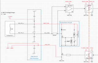
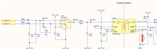
I'm using the INA180-Q1 (A version) in an automotive application in differential amplifier configuration for a high side current measurement. 

The sense resistor (22 mΩ) is connected between the positive and negative input signals. The common mode voltage is typically 12V from the battery. 

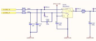
We observe that INA180 is destroyed at common mode voltages higher than 5V. According to the datasheet, the common-mode range is 28V max. 

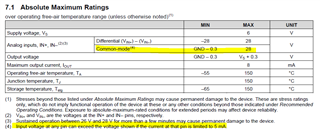
1- Does this behavior have anything to do with missing input current limitation? (See note 4 in absolute max. ratings). Do the input terminals need current limiting resistors?

2- I'm not sure how the input pins could draw more than 5 mA. The internal input resistors are specified as 25 kΩ according to Table 1. Input Resistance of datasheet. Do you have input protection diodes in front of the internal resistances which might be conducting high currents? Can you provide me with a more detailed block diagram? 

Thanks in advance,

Utku Karakas

  • Hi Utku,

    can you scope the input lines? You probably suffer from inductive kick back. Can you tell something about the load? Is it inductive or is any cabling involved.

    Have you tried the protection circuits shown in figure 49 and 50 of datasheet?

    Kai

  • Hey Utku,

    Welcome to the forum.

    The INA181 should always work properly (and definitely with no current-limiting input resistors) within the specified operational common-mode range (0V to 26V)..

    There could be a set up issue. One potential issue we see is a ground loop condition if all grounds are not connected with low-impedance connections. If the battery negative terminal and the ground of the INA180 are not connected/common, then this could cause an issue and violate the VCM of the device.

    Could you double check this and provide some more information:

    1. What is happening when the INA180 is destroyed?

    2. Schematic, test set up

    3. VCM and Vout measurements with respect to the INA180 ground.

    Sincerely,

    Peter

  • Hello Peter & Kai,

    Thank you for the quick feedback.

    Problem definition:

    When we turn on the 12 V battery voltage supplying the contactor (the PWM MOSFET driving the contactor current is still OFF at that moment), one of the following 2 things happen:

    1. either the input filter resistors (10R) are destroyed due to high current (we measured them to be very high ohmic)

    2. or the INA180 gets destroyed before the input filter resistors are destroyed first

    So we are guessing that somehow too much current is flowing into the inputs of the INA180. We are using 2 isolated output channels from the laboratory power supply:

    One channel for contactor 12V(VBAT3)/contactor ground(GND_CON) and the other channel for 12V supplying the controller circuit (CL30)/controller gnd (CL31).

    Unfortunately I don't have any measurements right now, because my collegues found a dirty fix by increasing the 10R filter resistors to 6k2 due to deadline constraints, which seems to work. We know that this fix is worsening the gain error a lot but it is compensated this in the next OPAMP stage.

    Here is the block diagram of the circuit:

    The INA180 output is fed to an isolation amplifier, because we use seperated grounds between the contactor side (GND_CON) and the main controller circuit side (GND). GND_CON is the reference for VBAT3, which is supplying the contactor. The protection circuit shown is the recommended design of our contactor supplier.

    INA180 & ISO Amplifier stage. The iso amplifier output is fed to an OP AMP which is amplifying the voltage further. That signal is connected to the ADC of the microcontroller.

    The PWM digital isolation and gate drive circuit:

    Gate drivers outputs are connected to the lower PWM MOSFETs.

    Thanks in advance

    Utku

  • Hey Utku,

    I don't see anything blatantly wrong with the schematic, but there must be some ground loop bug in the hardware. You can check by measuring the resistance between all of the ground nodes, especially the battery negative terminal and the INA180 GND pin. Go around the board probing with a DMM for high resistance between all of the grounds. 

    It could also be possible that the input ESD cells of the INA180 were damaged during handling and are conducting high currents once voltage is applied. You can try another system with a new, unused, working INA180 to test if the root cause is damaged ESD cells or if it is a ground loop. Or you could solder on a new INA180 onto the same PCB, but ensure proper ESD handling precautions.

    Finally, before you re-test anything, I recommend connecting an oscilloscope probe to the input pins of the INA180 with respect to INA180 ground pin. It doesn't seem likely, but there could be a large input VCM transient spike that could be also damaging the device's input ESD cells. This could help prove root cause.

    Best,

    Peter

  • Hi Utku,

    yes, you will need to make measurements with the scope directly at the inputs of INA180 relative to its ground pin. And I'm sure you will see insane voltage spikes either going negative or exceeding the positive common mode input voltage limit.

    Perform the measurements by using such a ground spring:

    Kai