This thread has been locked.

If you have a related question, please click the "Ask a related question" button in the top right corner. The newly created question will be automatically linked to this question.

XTR117: Is 4-20 mA output port considered as symmetric or asymmetric?

Part Number: XTR117
Other Parts Discussed in Thread: ADS114S06
Hey everyone,
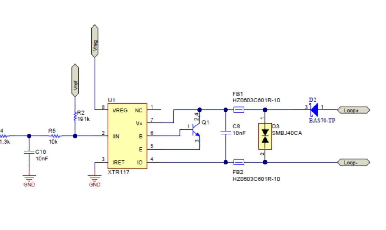
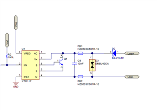
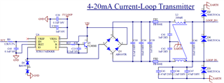
We are testing a 4-20mA transmitter for EMI/EMC compliance. The product has just one port where the device is connected in the following manner. 
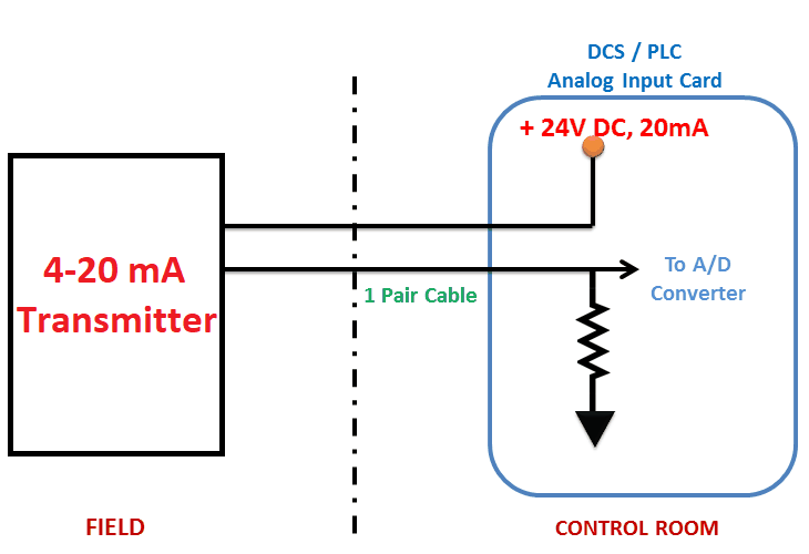
As you can see the device just controls the flow of current depending on the process value. 
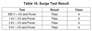
While referring to 61000-4-5 standard for surge test. The test setup depends on if the port is symmetric or not. 
The issue we are having is understanding if the 4-20 mA is symmetric lines or not?
The definition is given as " symmetrical lines pair of symmetrically driven conductors with a conversion loss from the differential to the common mode of greater than 20dB"
Other definitions online deal with voltage signals without commenting anything on the current signals.
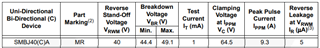
We are using XTR117 for controlling the 4-20 mA line. The testing information provided by the TI doesn't go into much detail about the same. Also, the surge applied in the TI's application note is always differential surge (given between loop +ve and loop -ve) while in the 61000-4-5 standard it is said to be tested as a common mode surge (given to loop +ve and loop -ve at the same time with respect to Power Earth)
Anyone who has tested such equipment it will be very helpful if they can guide us.
Thank you! 
  • Hi Yash,

    yes, the 4...20mA lines might be considered as twisted pair, but nevertheless it's not symmetric. I cannot see the typical chracteristic of a differential or balanced signalling (what you would call "symmetric") as both lines see different impedances. One line is driven by a zero impedance 24V power supply while the other line goes into a burden of medium impedance like a 500R load. e.g.. So I would treat them as unbalanced lines according to this nice pdf:

    7875.4_Transient_immunity_testing.pdf

    Kai

  • Hi Yash,

    Enclosed is TI's IEC 610000-4-5 test procedure and definitions. The 4-20mA current loop is definitely not balanced, hence you may consider it as asymmetrical communication line. I read Kai's comments, which I tend to agree. 

    Let me consult with our expert and get it back to you, because there are many definitions in this test category, some are more general; some are addressed specifically for high speed communication etc.. XTR117 is a low communication or near DC 4-20mA current loop, and it is unidirectional. 

    https://www.ti.com/lit/an/slva711/slva711.pdf?ts=1630534753193&ref_url=https%253A%252F%252Fwww.google.com%252F

    Best,

    Raymond

  • Hi Yashi,

    The issue we are having is understanding if the 4-20 mA is symmetric lines or not?

    We have confirmed that the 4-20mA current loop in XTR117 part shall be treated as asymmetric lines per IEC 610000-4-5 compliance test, please see the test procedure enclosed in the prior reply. 

    If you have additional questions, please let us know. 

    Best,

    Raymond

  • Hi Yashi,

    One more thing to add, you may want to consider performing both the common mode and differential surge tests. The TVS diodes across the loop supply line and Iout line will be your main line of defense against a differential voltage, while the entire circuit (XTR, downstream circuitry, etc) should theoretically float when the common mode test is applied. There will be a certain degree of differential voltage that occurs since the CMRR of the device is not ideal, but again that's what the TVS diodes (and bypass cap) are there for. 

    As Raymond said our testing in the past has made use of the 1.2/50µs CWG waveform one would associate with asymmetric lines, and it does seem as though the wires fit the definition of asymmetric lines, but at the end of the day the test specifics and pass/fail criteria will depend on what the person or team defining the product and associated tests determines is needed for compliance. Obviously a more robust, well protected system will usually be preferable so if it passes both common mode and differential surge tests then it's all the better, but it depends on what you decide is necessary.

    Cheers,

    Jon

  • Thank you all! your answers have cleared many things. 

    Finally, I want to know the TVS selection logic TI has used in "Digitally Calibrated Bridge Sensor Signal Conditioner with
    4mA to 20mA Current Loop Output

    So TI has used SMBJ40CA in the above design, which passes the 5kV surge test as shown below. 

    I have two concerns with the selection 

    1. The clamping voltage (64.5V) is higher than the XTR117's absolute max of 50V

    /

    2. The calculation for the above-mentioned TVS diode shows it can take around 27A max with 42Ω in series for an 8/20uS surge. How has TI passed the 5kV surge which will require 119A for 42Ω in series? Am I doing my sizing calculations wrong? or have considered the wrong series impedance.

  • Yes Kai, I remember and it was very helpful. But as per your answer you said 500V is the max rating hence the SMBJ made sense.

    But again as mentioned in above thread the TI's design passed 5kV. 

    Also, I am asking this question again is because I want to understand the calculation behind it.

  • Hi Yash,

    this must quite obviously be a mistake. No one has to surge test signal lines up to 5kV. 500V L-L and 1kV L-E are the standard levels, as I said before.

    The BAS70 cannot withstand 5kV / 42R = 119A either. This is ridiculous.

    Kai

  • Hi Yash,

    I think this is an error as well, the SLVA711 document on IEC 6100-4-x specifies test voltages of 500V, 1kV, 2kV, and 4kV (see page 7) so I can only assume that 4kV was the actual test value. This would be 96A surge. See also Table B-6 from the TIPD user guide, which mentions 4kV and 95A.

    Regarding the clamp voltage, it appears the design was intended to support a loop voltage of 40V, so a decision was made to go with a higher clamp voltage than we would otherwise recommend in order to get a higher breakdown voltage (see page 8 of the TIPD). If you only anticipate having a maximum Vloop of 24V (let's say 30V to give some margin), it would indeed be a good idea to go with a TVS that has a sub-50V maximum clamping voltage, like the SMBJ30A or similar.

    Regarding the surge current, keep in mind the datasheet for that TVS specifies the power limits for a 10/1000us waveform and the peak forward surge current for a 8.3ms single half sine wave, duty cycle 4 per minute maximum. I would not be surprised if it can handle much higher surge currents for the 8/20us waveform due to the shorter duration. 

    Cheers,

    Jon

  • Hi Yash,

    as I recommended earlier, we use the 1.5KE36CA or SMCJ30CA in a similar application being powered from the +24V supply of process control. The threshold voltage of said TVS is +30V which is 25% above +24V allowing the +24V supply of process control to have some tolerances.

    Instead of the BAS70 take a robust rectifier diode which not only allows the surge current to flow but also shows sufficiently high maximum reverse voltage. Or mount the diode behind the TVS.

    Kai

  • Hi Kai, I am a part of Yash's team on this project. After this thread, we modified our design as such

    However, very strangely, on applying 1kV L-E (balanced, all lines to earth), we find that the surge damaged the XTR and our microcontroller while simultaneously leaving both the L-E TVS diodes untouched. This is baffling, but perhaps the following EMI filters we have in another section of the schematic might be allowing the surge to bypass the TVS and couple from the chassis earth into GPIO pins of the microcontroller?

    We're also failing the conducted RF test at ~45 MHz with 3V test level. Somehow the noise couples to our ADS114S06 input pins, but since it is common mode noise, the CMRR of the ADS should have removed it, correct?

    If it provides another clue, we have the same EMI filter protection on the ADS114S06 input pins. We can try removing those on our next test day and see if it helps.

  • Hi Gaurav,

    the mistake is that you have placed TVS diodes from signal and DC power lines to protection earth. Never do this, as then you force Surge currents through signal ground connections where never a Surge current would flow, normally.

    Only connect TVS diodes from signal and DC power lines to signal ground and -if necessary- bypass signal ground to protection earth via 10nF/1kV caps. When L-E Surge testing no Surge current will flow into the 10nF/1kV cap then, only a charging current which does not last very long and can easily withstood.

    If there is accidentally a TVS from signal ground to protection earth at some place (which no professional industry electronic circuit has for very good reason !) you would need to strengthen all involved protection circuits which can really become a mess. So, never connect a TVS from signal and DC power lines to protection earth. Connect it between signal and DC power lines to signal ground, and -if necessary- bypass signal ground to protection earth via a 10nF/1kV cap.

    Keep in mind that the XTR117 and similar products are designed for being totally isolated from protection earth at the sensor side (where the XTR117 sits). The shunt and the 24V supply at the receiving side might be referenced to protection earth when being powered from a PELV. But not at the sensor side!

    Keep also in mind that the "Iret" pin and other pins of XTR117 is no signal ground. They might work as such in the circuit, but in truth they are fully floating and cannot absorb ground return currents form other circuitry or currents flowing into a shield "provisionally" connected to the "Iret" pin. "Iret" and most other pins of XTR117 are ultra sensitive and susceptible nodes. This means that the sensor side must be kept well away from protection earth or objects being connected to protection earth to even minimze stray capacitance to protection earth. But then the XTR117 is totally immune against Surge!

    But don't make the mistake and connect something to the input of XTR117 which again has some connection to protection earth and ruins this full isolation from protection earth. You will very probably fail most of CE testings then.

    Some words on your common mode filter L2. Common mode filters often do more harm than good. I would always omit a common mode filter unless there's an absolute need for it. In any case a common mode filter with Y-caps being connected to protection earth should never be used at the sensor (XTR117) side. Keep in mind that an Y-cap not only shunts EMI to protection earth, which would be good, but it can also inject EMI from protection earth into signal ground. This might not be a problem at the receiving side, but at the sensor side it can mean a disaster.

    Kai

  • Dear Kai,

    Thanks for the detailed response. If I understand you correctly, we need to remove the Y caps to earth (C41/C42) and the TVS diodes to earth (D2/D3) and try without the common mode choke. We will implement these changes for surge and conducted RF.

    However, I have just one doubt, and that is regarding ESD. If I understand right, the aim of the game is to shunt all ESD into the metallic chassis as far away from sensitive parts of the circuit as possible, correct? And then the PE connection would bleed out the charge slowly bringing the enclosure back down in voltage.

    For all direct discharges into the body or via horizontal/coupling planes, I understand the metallic chassis stray capacitance to ground will draw the charge. Once the enclosure charges up to a few kV, how do I protect the circuit inside from a possible secondary arc without a strong connection from enclosure to the signal ground somehow? The original intention was TVS from line to ground so that they would breakdown and float the circuit up through LOOP + and - instead of building up enough potential difference to possibly cause a secondary arc.

    Also, for air discharge near the keypad buttons/LCD display pins, the TVS diodes on the microcontroller GPIO pin (like inside U9 in my previous comment) need to shunt the ESD to ground somehow. Do I connect them to the chassis ground (and ruin isolation of the circuit for surge) or into signal ground (and risk damaging the sensitive Iret pin of the XTR117)

  • Hi Gaurav,

    yes, I would remove L2. FB1 and FB2 should be enough HF filtering. You can additionally thread the both lines running to the XTR117 through a ferrite ferrule forming a common mode choke. And you can mount such a ferrite ferrule at both ends of the cable. But I would not use a common mode filter with Y-caps.

    D2 and D3 can make absolutely sense. But only if they are referenced to signal ground or DC power ground. The "LOOP IN+" terminal will go to the +24V supply, right? Having a TVS here is a good idea. But please not referenced to protection earth!

    And "LOOP IN-" goes to the burden (load), right? Here again a TVS can make sense to protect the shunt and the following electronics. But please reference the TVS to signal ground and not to protection earth. Signal ground might have a direct connection to protection earth here, when a PELV is involved, for instance. This is ok. But don't make an abitrary connection to protection earth, just for the case that there is no connection from signal ground to protection earth for some good reason.

    There's also an issue with C45, C46 and C47. You should not have so much capacitance at this place, neither to protection earth nor to signal ground. Why we don't want to have capacitances to protection earth I have discussed above. But even if D3 would be referenced to DC power ground or signal ground, such a high capacitance is counterproductive because it would appear in parallel to the burden. I would mount a 10nF capacitor in parallel to the shunt, if at all, and add an additional RC low pass filter behind. This gives a much better low pass filtering than a big capacitance across the burden. And the output of XTR117 does not need to drive into a capacitive short-circuit by this measure.

    Once the enclosure charges up to a few kV, how do I protect the circuit inside from a possible secondary arc without a strong connection from enclosure to the signal ground somehow?

    The inside of a Faraday cage is free from electrically fields. The electrons in the Faraday cage move and generate an eletrical field which exactly cancels the electrical field from the outside. If the canceling effect is not yet optimized, they move as long as the cancelling is perfect. If a lightning is hitting your car you can safely touch the inside of car chassis.

    If ESD is hitting a metallic enclosure, all ESD current is flowing on the outside layer of the metallic enclosure. The skin effect makes that the ESD current is flowing within a microscopically thin layer on the outside of metallic enclosure. No current is flowing in the inner side of metallic enclosure. A capacitor connected to the inner side of metallic enclosure would not conduct anything of this ESD current into the inner of metallic enclosure.

    This is what's going on in an ideal Faraday cage. In a non-ideal Faraday cage the inner of Faraday cage might not be entirely free of electrical fields. Yes, it is true that connecting signal ground to the metallic enclosure via a cap can force signal ground and metallic enclosure being at the same potential. But just this can do more harm than good, if a relevant portion of ESD current is now injected into the electronic circuit which would not be injected otherwise only by the unavoidable but low stray capacitance.

    Also, for air discharge near the keypad buttons/LCD display pins, the TVS diodes on the microcontroller GPIO pin (like inside U9 in my previous comment) need to shunt the ESD to ground somehow. Do I connect them to the chassis ground (and ruin isolation of the circuit for surge) or into signal ground (and risk damaging the sensitive Iret pin of the XTR117)

    Never allow ESD to enter the electronic circuit and run over the printed circuit board. If this happens, you are lost. Always shunt ESD to the outside of metallic enclosure (or suited radio frequency plane, if an metallic enclosure cannot be used). Physics helps you by the skin effect and the mechanism of Faraday cage. ESD always searches for the best path to soil, which automatically is the path of lowest inductance. And this is the outside of Faraday cage and cable screen, if you will only allow this. ESD does not want to enter a circuit, but it will when there's no other way to find the soil.

    The metallic enclosure must not be connected to protection earth -and certainly not by a piece of wire- to be a powerful tool against ESD. ESD running on the outside of Faraday cage finds soil just automatically via stray capacitance. The metallic enclosure even must not be connected to signal ground to work as a shield against ESD. Of course, for other EMI purposes you want to have the metallic enclosure being connected to signal ground, at least for HF, via hybrid grounding.

    Still one last point on Surge: If you connect the metall anclosure to protection earth and have signal ground and the whole electronics being connected to the metallic enlosure by a 10nF/1kV cap (also called hybrid grounding), then in the event of 1kV L-E Surge the whole electronics will move for some tens of microseconds 1000V away from the potential of metallic enlcosure. The electronics must be able to withstand this. For instance, by using individual internal shieldings which are connected to signal ground and by using suited isolation at vulnerable points to prevent arcing overs from the electronics to metallic enclosure (or vice versa). But all this can far more easily be handled than a Surge current of tens of Amperes unwantedly flowing through the electronics.

    Kai 

  • Dear Kai,

    yes, I would remove L2. FB1 and FB2 should be enough HF filtering

    Don't FB1, FB2 and the capacitors form a differential filter? If L2 is gone, I am wondering what would attenuate the common mode noise injected from 0.15 - 80 MHz. Is this the job of the CMRR of the ADS114S06 to eliminate this noise? Or if it couples to the Iin of the XTR, I would see the loop current fluctuate, right?

    There's also an issue with C45, C46 and C47. You should not have so much capacitance at this place

    Those aren't populated (and should have been marked that way). They're just there on the PCB for us to have options at the time of EMC testing. Also, we don't have access to the power supply or burden side of the system, only to the sensor side.

    D2 and D3 can make absolutely sense. But only if they are referenced to signal ground or DC power ground. The "LOOP IN+" terminal will go to the +24V supply, right? Having a TVS here is a good idea. But please not referenced to protection earth!

    And "LOOP IN-" goes to the burden (load), right? Here again a TVS can make sense to protect the shunt and the following electronics. But please reference the TVS to signal ground and not to protection earth.

    I have access to just the signal ground and protective earth (through the chassis connection).
    I thought that since the surge is applied w.r.t. protective earth, and chassis earth is connected to protective earth, perhaps I would need TVSes w.r.t. protective earth. 

    The metallic enclosure must not be connected to protection earth -and certainly not by a piece of wire- to be a powerful tool against ESD. ESD running on the outside of Faraday cage finds soil just automatically via stray capacitance. The metallic enclosure even must not be connected to signal ground to work as a shield against ESD

    Of course, we would not be connecting the enclosure to signal ground, but based on our research of competing products, it is industry standard procedure to connect the enclosure to protective earth for transient protection and the cable screen near the power supply end. Please see the below snippet from a product installation manual.

    For ESD, we're trying to emulate this condition from Dr. Ott's book by having the metallic enclosure be grounded and the circuit be floating, so as to make a secondary arc occurrence extremely unlikely.

    But all that works perfectly except in the case of air discharge near the LCD segment pins and keypad buttons. So if I connect TVS diodes from the LCD segment pins and keypad GPIO pins to discharge to the chassis earth, then the ESD would not run through the circuit, right? This is the case currently, and we have zero issues with ESD damage. However, our device fails in surge, and I suspect that our ESD mitigation TVS diodes break the circuit isolation to protective earth and provide a surge path to damage the XTR.

    Would it satisfy both ESD and surge requirements if I were to connect the GPIO pin TVS diodes to signal ground instead of chassis earth, and to add hybrid grounding from signal ground to the protective earth. That way, the hybrid ground would shunt the ESD while blocking the surge.

  • Hi Gaurav,

    it's difficult to make comments on a product which I don't know at all. So I cannot make very specific comments on the LCD and keypad buttons. Usual measures are shunting ESD by the help of 100p...1nF caps from vulnerable points to a solid ground plane and from this back to the enclosure via 100p...1nF caps again. But TVS should not be used here, as this would create a path for Surge, as you mentioned.

    There's no need to connect the metallic enclosure to protection earth, unless the product contains safety class I components. And even if so, there's no need to also connect signal ground to protection earth, unless a saftey class I mains transformer is used. But usually, you take a safety mains transformer which is safety class II. Then there's no need at all to connect signal ground to protection earth.

    Please see the below snippet from a product installation manual.

    Don't rely too much on these installations manuals. Many of them contain old school methods which are no longer valid. And there are many different philosophies arround which are excluding each other and don't fit together. In the early days the cable screen was only connected on one side to prevent hum loops. But today we have learned that we can no longer do this with all this heavily increased EMI (cellphones, ...). Today we run signal lines in shielded cables with the shield being bonded to protection earth at both sides where the cables enter and leave the control cabinet. Signal ground is freely floating and is connected to protection earth only via 10nF/1kV caps, but never via a TVS.

    Kai


  • Kai,

    There's no need to connect the metallic enclosure to protection earth

    If the entire device is mounted onto a larger grounded system with metallic bolts, I don't think I'd be able to isolate the chassis from earth.
    I wouldn't want to certify a floating device only to find out from the field that devices are failing due to the chassis mounting connection creating an earth path.

    Nonetheless, in our first test, we had failed ESD but passed surge without the L-E TVS diodes and caps. This was irrespective of whether the chassis was grounded or not.

    In our next test, grounding the chassis and adding the above components L-E, we passed ESD without a hitch, but failed surge.

    So keeping the chassis grounded, we're going to try out what you said and I will get back to you once I have the results.
    All TVS would be GPIO to signal ground instead of chassis ground, and we would have hybrid grounding from signal ground to chassis.

    Kai, you have been extremely helpful and I thank you for the valuable support you have provided.

  • Good luck Relaxed

    Kai