This thread has been locked.

If you have a related question, please click the "Ask a related question" button in the top right corner. The newly created question will be automatically linked to this question.

OPA455: the current is step by step

Part Number: OPA455
Other Parts Discussed in Thread: OPA2191

Hello, TI  Expert :

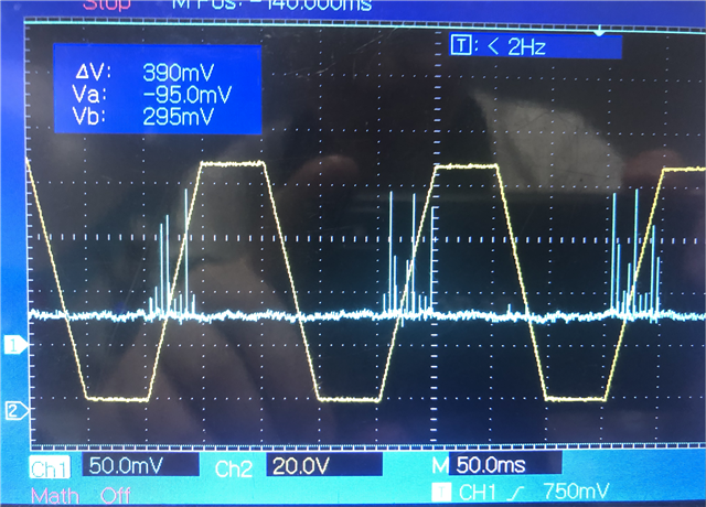
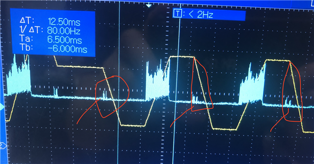
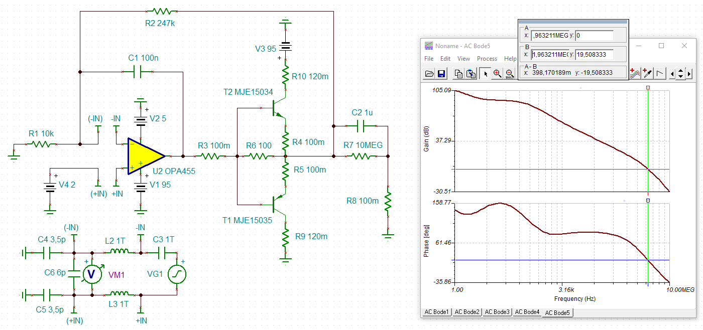
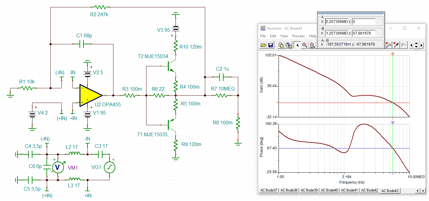
   1.I am using OPA455 to extend the current , below is the sample schematic. I am confuse the current waveform, why it will occur the pulse current . Can you help share the technology knowledge .    

   2.The DAC output is 50 point to reached 0V – 3.3V the OPA455 gain is 29, so the output voltage 95.7V.

01_source_0913.pdf

  • Does "PN5V" mean -5V? Otherwise you will violate the common mode input voltage range of OPA455.

    Why is the signal at the input of circuit "0V-2.5V" and later at the +input of OPA455 "1V-3.5V"?

    Where in the circuit the current shown in the scope plot is measured?

    Is the OPA455 becoming warm or even hot?

    Kai

  • Hi,

    In addition to Kai's questions is it the spikes on the white O-scope trace (ch1 - output current?) that are what you are asking about? I assume that the yellow waveform is the OPA455 output voltage?

    Regards, Thomas

    Precision Amplifiers Applications Engineering

  • Thanks Kai and Thomas for your kindly reply

    1. The blue CH1 is the current probe I measure the current in the PP95V line, The yellow CH2 is measured at T3 test point.

    2. Does "PN5V" mean -5V? Otherwise you will violate the common mode input voltage range of OPA455. 

       >>> yes! it is -5V.

       Why is the signal at the input of circuit "0V-2.5V" and later at the +input of OPA455 "1V-3.5V"?

       >>> it a clerical error, the OP is work follower, the +input of OPA455 will be  "0V-2.5V", or will change to "0-3.3V" according the DAC reference voltage.

     Is the OPA455 becoming warm or even hot?

      >>> The OP work very well.

    3.The previously schematic, I didn't add the Q3 & Q4, I measure the high side current at R2, the rising edge can measure large current , the falling edge also can measure some current at R2. I think the falling edge the R2 current should be ZERO, because the capacitors is discharge the voltage and current. I don't why the falling edge can measure current ?

    4.I use DAC to generate the rising edge and falling edge, so there is some vertical step of the output voltage, can you recommend some suggestion to make the output wave more smooth? The rising edge time is between 0.1ms and 3000ms, same the falling edge time. 

  • Hello Thomas,

    Based on your number 3 item the OPA455 circuit does however include the Q1 and Q2 power transistors in the feedback loop. They appear to be operating as a class B follower stage. It's possible the loop is becoming unstable at points as the bias on the output transistors changes with the DAC voltage.

    Have you tried this same test without Q1 and Q2 in the circuit? I realize you wouldn't be able to drive the high current, but we need to know if the OPA2191/OPA455 circuit has a clean output on its own.

    Regards, Thomas

    Precision Amplifiers Applications Engineering

  • If the circuit becomes instable when the DAC output changes, as Thomas mentioned, then a low pass filter at the input of U4A should help. Mount a cap from test point "T2" to signal ground.

    (Without having performed a phase stability analysis) C5 looks a bit weird to me. I think 100nF is a bit high. High capacitances can be counterproductive in a feedback loop. You wouldn't want to have a short circuit at the higher frequencies in the feedback loop in most cases, but only some phase lead to compensate for unwanted phase lag. I would check, if a much smaller C5 will also do. Start with some tens of pF and increase, if necessary.

    Have you already performed a phase stability analysis?

    Kai

  • It turns out that your circuit instable:

    xing_opa455.TSC

    I would give these modifications a try (C1 and R6 in my schematic):

    xing_opa455_1.TSC

    Kai

  • Dear Kai and Thomas thank you very much for your kindly reply.

    1.According your suggest I will change the C1 and R6 value, But it need time to buy it.

    2.There is an other question how to select the RC low pass fillter? Please kindly check the attached is contain more details。

    OPA455_0917.pptx

  • Kai,

    Thank you for the complete stability analysis of Xing's OPA455 circuit. Let's see what Xing finds after the C1 and R6 revisions.

    Xing,

    Is the RC low-pass for the DAC output? Such a filter is referred to as a DAC reconstruction filter, or anti-imaging filter The design of such filters is quite involved and usually requires more than just a simple RC filter. Here is a link to a TI DAC Precision Labs training session on the subject:

    https://training.ti.com/sites/default/files/docs/TIPL4705%20-%20DAC%20Output%20Response.pdf

    This filter looks like it can be a very difficult part of the overall design. Here is a TI Analog Engineer's Circuit about active filtering for an audio DAC that might be usable for your application:

    https://www.ti.com/lit/an/sbaa322/sbaa322.pdf

    Regards, Thomas Precision Amplifiers Applications Engineering