This thread has been locked.

If you have a related question, please click the "Ask a related question" button in the top right corner. The newly created question will be automatically linked to this question.

OPA657: OPA657 Noise calculation as TIA

Part Number: OPA657
Other Parts Discussed in Thread: OPA818, OPA2320, LM4132, TINA-TI, OPA320, OPA627

Hi team,

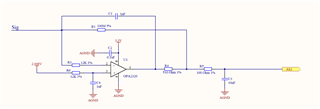
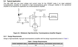
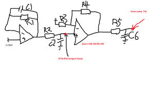
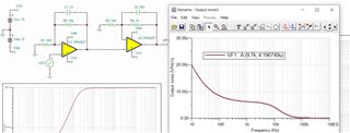
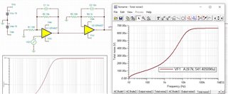
I want to use OPA657 as a TIA circuit. I need to calculate the noise for OPA657 TIA circuit. 

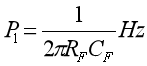
Q1: In the datasheet, I cannot understand" Equation 9" as below:

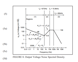
What is the F value in Equation 9 ? F=f =sqrt(GBP / 2 R C) Hz

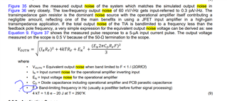
Q2: How to calculate CD in Equation 9?

  • Morning Mr. Zhang, 

    That equation came out of some work I was doing back inthe 1996 time frame - published in a series of articles, but summarized in this design presention - those articles are referenced in the end of this, the theme of this treatment is to make judicious simplifications to get accurate results with far less complexity in the equations. 

    4331.Transimpedance design flow using high speed op amps.pptx

  • Hi Michel,

    Thanks for your PPT.  But I cannot still understand the output noise calculation. Can you help me? I need to confirm the below information as below. Can you help me? 

    Q1: For OPA657  Equation 9,  The max F value=  ?

    Q2: When I calculate OPA657 the output noise  and  Equation 9 of OPA657 datasheet, If the calculated value is A, What is the Unit of calculation for A? Is it V/sqrt(HZ)?

    Andthe total output voltage noise=A*Sqrt(Ln(the Noise Bandwidth)? 

    And How to calculate the Noise Bandwidth?

  • Equation 9 is setup assuming a bandwidth limiting filter after the transimpedance stage to control the noise integration span. If you let the stage bandlimit on its own, the equations are much more complicated and you usually have filtering after this stage that you can lean on to define the noise integration BW. Noise power bandwidth is another discussion but for instance a single pole RC will have a noise power bandwidth of 1.57*F-3dB bandwidth. 

    The units of equation 9 are V/rootHz - if you input refer by dividing by Rf, it is A/rootHz. 

    There is in fact an upgraded part lo the OPA657 - the OPA818 - I don't see this noise equation in there (?), but it does apply as well. 

    If you want a more wide ranging noise analysis discussion, that is here - this one came out of years of noise analysis I had been doing starting from the Motchenbacher and Fitchen book from the mid 80s onward. This was a BurrBrown app note I was writing at the same time I was doing those transimpedance design articles on EDN

    https://www.ti.com/lit/an/sboa066a/sboa066a.pdf

    If you have a specific design requirement, I could perhaps step through a TINA example. But time presses, good luck.

  • Oh and incidentally, that "F" which is the span of noise integration defined by a post filter has to be < than the feedback pole frequency for the equation to work. This makes sense application wise as that pole frequency is set for the desired response shape - but the Zt stage itself will have quite a bit of variability due to gain bandwidth product variability - to get more design control, it is better to set the Zt nominal BW beyond what you need and then control the final result with a postfilter showing lower variability at less than the Zt stage nominal BW. When I was running that integral to get the noise, I only ran up to some F that is on the rising portion of the noise gain curve - if you go on out from there to the feedback pole then the LG =0dB intersection, the equations get beyond what was willing to take on. 

  • Yes, I have a TIA circuit. Use OPA2320. The min input current is DC 1nA. Would you help me to analysis the output voltage noise? 

    2.048V is output by LM4132.  I think OPA2320 Output noise should include the 2.048V REF noise, correct?

    By the way,  I found the document: sboa060. It shows the TIA circuit noise calculation. But I do not know what f3 80KHZ is? Would you check this?

    sboa060.pdf

  • So that even older BurrBrown noise app note is including all the regions of a self limited transimpedance design - it is this level of complexity I was trying to simplify using actual full system concepts including postfiltering - your circuit looks like it needs correcting, but the TI team is poised to handle that I am sure. 

  • My circuit is  not correct? Would you help me to analysis the output voltage noise? 

  • Hello Tengfei and Michael,

       Thank you Michael for the additional noise references and explanation. 

       We could help fix your circuit. The basic TIA circuit looks similar to the one provided in the device datasheet:


       Would you be able to provide us with the photodiode's internal capacitance, the photodiode's current range, and the output voltage range you need out of the amplifier?

    Thank you,

    Sima

  • I don't use  photodiode in my application.  I think my application do not have the  internal capacitance.The input current range is 1nA~20nA, TA:-40C~60C. 

    The output voltage is  about 0~2.048V. Not I want to get how to  calculate TIA circuit  noise. Would you help me to do this?

  • Hello Tengfei,

       Michael shared earlier content on this. But, I can share additional references which go through a specific example using a TIA. I would double check if you input source has some sort of internal capacitance, but you can estimate CD (diode capacitance) to be from parasitic of PCB. Input capacitance will need a small compensation feedback cap. 

    1. Noise Analysis of FET TIAs (goes through total noise which includes current, voltage, and resistor noise)

    2. TIA Noise Analysis PowerPoint (also goes through total noise, but more detailed with TIA noise example and simulation) attached below

    3. Written PDF format of the PowerPoint; chapter 11 and chapter 12 attached below

       Let me know if you have any questions from these documents. You can also simulate this in Tina-TI which can produce plots of the circuit's output and total noise which is covered in this video. I would highly suggest simulating your circuit. It looks like you are using an in-loop compensation technique to reduce bandwidth and effectively the noise. But you also have a isolation resistor at the output, you can remove the compensation in the feedback and inner loop, and just use RC filter at the output of the amplifier. 

    Noise In Photodiode applicaitons_Art Kay.ppt

    noise11-Photodiode-Noise 1.pdf

    noise12-Photodiode-Noise 2.pdf

    Thank you,
    Sima 

  • Hi Sima,

    I have get the TIA noise calculation.  In my application, I have estimated my TIA OPA320 circuit  output noise= 480uV.  It is  a lagre value. 

    I want to use RC low pass filter to reduce the noise. 

    1. I want to confirm the Noise Bandwidth when I use RC low pass filter on OPA320 output pin. The new Noise Bandwidth=1.57*1/(2*3.14*RC)?

    2. If the 1st step is correct, I can use the new Noise Bandwidth to recalculate the OPA320 Output noise? 

    I can use  the new  Noise Bandwidth instead of  the formula Noise Bandwidth for PPT page41- page44? Then get a new output noise.

    3. In my application, I need to use the TIA output value to as the input signal to design a G=100 phase amplification.

    If TIA OPA320 output total noise=100uVrms, How to calculate the output noise for only TIA as the input voltage?

  • Hello Tengfei,

      Yes exactly, a RC low pass filter will reduce the system bandwidth which will effectively reduce the noise. 

    1. That is correct, it would be the one pole filter estimation (1.57) * noise bandwidth of the system which is 1/2piRC. 

    2. Yes, then you use this noise bandwidth to calculate 1/f and broadband noise which its combination will give you total voltage noise. Then you can calculate current noise and resistor noise, which will give you the total noise of the system. Pages 41-44 in the PowerPoint is the same concept, but includes noise of the current source (photodiode) and uses the transconductance bandwidth.

    3. I don't think I quite understand this question. Is the TIA a gain of 100, or is there a following stage that is a gain of 100? 

    Thank you,
    Sima 

  • Smia,

    You may check the below circuit:

    R5=1K, C6=0,1u The second amp Gain=100, If TIA output noise=VITA=480uV,

    I want to get  R5 C6 Output noise that is only TIA noise 480uV is as a input noise.  1/2*3/14*1K*0.1u=1592HZ, fnoise banwith=1.57*1592=2500HZ,

    SQRT(2500)=50

    R5 C6 Output noise= 480uv*100*50 ? I think this is incorrect,but I don't know how to calculate.

    If the circuit has 2-stage amplification,I don't know how to calculate the output noise that is in the 2cd amp output.

  • Hi Sima,

    Would you confirm this question?

  • Hello Tengfei,

      Sorry for the delay in response. For a multi-stage amplifier design, the noise from the first stage will be amplified in the next stage. This is why we always recommend to design your application up to the highest gain up to the minimum bandwidth requirement, then add the rest of the gain in the following stages. 

      To calculate the total output noise of the system, you need total rms noise from stage 1 and from stage 2. For intensive calculations, this will include voltage noise (broadband), current noise, and thermal nosie. The square root sum of the squares of each term will give you the total V/sqt(Hz). This can be simplified by taking the most dominant term. Then to get Vrms, you multiply this term to the noise bandwidth which you already have calculated. 1/f term can also be added here. 

     So let's take the total output noise of the first stage that you already calculated, 480uV. This term should have been nV/sqrt(Hz) which was multiplied by the noise bandwidth from the filter to give you the uV total output noise. Also you do not need RC at the output of the first stage, the RC in the feedback should suffice.

      This means x nV/sqrt(Hz)*sqrt(Kn*1/(2pi*R1*C1)) = 480uV RMS. This term is then multiplied to the noise gain of the second stage (101)

      For the second stage, you would repeat the same process using the noise bandwidth of the second set of filter (R5 and C6) to obtain the total RMS output noise including all components discussed above. Then multiply this term to the noise gain of the second stage (101). 

      Combine the output noise of first and second stage by square root of the sum of squares: sqrt(En1^2 + En2^2). 

      Michael has a really good article that goes over this exact situation: controlling spot and integrated noise in a two-stage transimpedance design

     Also, the TI precision lab on noise; specifically 8.4 goes over calculating the noise of a two stage amplifier design. Look at time-stamp 14:18 for a detailed step by step calculation of the total noise using the OPA627. 

    Thank you,

    Sima 

  • Hi Sima,

    Thanks. I mean I want to confirm the noise bandwidth for the first stage.  I don't know which the  noise bandwidth is. for the first stage.

    For the first stage, There are 2  noise bandwidth :Kn*1/(2pi*R1*C1)  and Kn*1/(2pi*R5*C5).

    For example, If the first stage output total noise is 100 nV/sqt(Hz),  The second Gain is G2, En1 is the output noise in the second stage for the first stage.

    (1) Kn*1/(2pi*R1*C1) =1K, Kn*1/(2pi*R5*C6)=100K, En1=G2*100nV/sqt(Hz)* 1K? Or En1=G2*100nV/sqt(Hz)* 100K?

    (2) Kn*1/(2pi*R1*C1) =100K, Kn*1/(2pi*R5*C6)=1K, En1=G2*100nV/sqt(Hz)* 1K? Or En1=G2*100nV/sqt(Hz)* 100K?

  • Hello Tengfei,

      In the earlier reply, I used the worst-case scenario for each stage similar to the method used in the TI precision lab video. Technically, this is not a first order system; but if we use the second to third order systems, it would under-estimate the output noise. 

      For a worst-case scenario, use the noise bandwidth of the first stage (1.57*(1/2pi*R1*C1)) to calculate output total noise of the first stage, and use the noise bandwidth of the second stage (1.57*(1/2pi*R5*C6)) to calculate input total noise of the second stage. 

      For a simplified worst-case scenario, use the noise bandwidth of first order system at the higher bandwidth: 1.57*(1/2pi*R5*C6).  This E2E thread goes over this in detail with simulation examples (attached below) based on the TI precision lab video example. 

    1134.OPA627 Noise.TSC

    Thank you,

    Sima


  • Sima,

    You said:

      "For a worst-case scenario, use the noise bandwidth of the first stage (1.57*(1/2pi*R1*C1)) to calculate output total noise of the first stage, and use the noise bandwidth of the second stage (1.57*(1/2pi*R5*C6)) to calculate input total noise of the second stage".  I don't quite understand.

    For the first stage output  total noise bandwidth in the second output pin=(1.57*(1/2pi*R1*C1))*(1.57*(1/2pi*R5*C6)) ? Could you explain in detail?

    I use 2 cases, In order to get the noise bandwidth for the first-level op amp  to calculate the first -level op amp  output noise while it is in the 2-level op amp output pin clearly.

    2 cases: According to your said, the calculation is as below, Are the calculation  Correct?

    (1) 1.57*1/(2pi*R1*C1) =1K, 1.57*1/(2pi*R5*C6)=100K, En1=G2*100nV/sqt(Hz)* sqrt(1K)? 

    (2) 1.57*1/(2pi*R1*C1) =100K, 1.57*1/(2pi*R5*C6)=1K,En1=G2*100nV/sqt(Hz)* sqrt(100K)?

  • Hello Tengfei,

      For that statement, I meant similar to method shown in the earlier image from the precision lab video, you can combine the output of first stage's noise with the input noise of the second stage's noise by calculating two output noise terms which is where two different noise bandwidth calculations come from.

     Multiplying the noise bandwidth together will not give the correct noise bandwidth. It is best to calculate for worst-case scenario which would be at a first-order system at the largest bandwidth, which in your case you calculated it to be 100kHz. 

      For both cases, in terms of calculation of En1 (output noise of 1st stage), 1) and 2) is correct. But case 1) in practice wouldn't make sense, since the bandwidth is already reduced in stage 1). 

    Thank you,
    Sima 

  • Hi Sima,

    Thanks for your assistance. And I also have a question. for your TINA circuit, 

     noise bandwidth :1.57*(1/2pi*10n*1k)=25KHZ, In the waveform: 25KHZ, noise output noise=1.6uV/sqrt(HZ), The total noise=641.9uV,

    1.6uV/sqrt(HZ)*sqrt(25000)=253uv. 253uv is not 641.9uv. Why is it not equal?

  • Hello Tengfei,

      To use the output noise from simulation, you will have to first check the cutoff frequency of the circuit by running the AC response:

      In simulation, the cutoff frequency is around 10kHz compared to estimated 1/2piRC of 15kHz. This is because in calculation we were assuming a first order system, but in reality there is a double repeated pole. The output noise of the second stage at 10kHz gives us around 4.2uV/sqrtHz:

      From there, we can calculate the total noise by the noise bandwidth: 1.57*(10kHz) = 15.7kHz. In reality, the k factor should be in between first and second order system. So, total noise calculation is: 4.2uV/sqrtHz * sqrt(15.7kHz) = 526uVrms. 

      Simulation gives us a similar number of around 541uVrms. 

    Thank you,
    Sima

  • Sima,

    Thanks a lot!