Other Parts Discussed in Thread: OPA188
OPA4188_config1.TSCOPA4188_config2.TSCOPA4188_config3.TSC
Hi,
I was performing noise analysis on below circuit using different configurations and hoping to match with the hand calculations, but it looks like I am missing something important.
Reference for calculation: "8.9 TI Precision Labs - Op Amps: Noise - Lab"
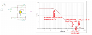
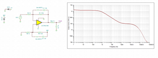
Config 1:
The results of hand calculation are matching with simulation as Vrmsnoise = 1.76uVrms
However, in the referred video, I noticed that, for thermal noise calculation only Rin is considered, not equivalent resistance. Can you please explain why?
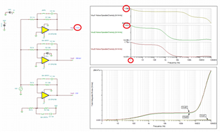
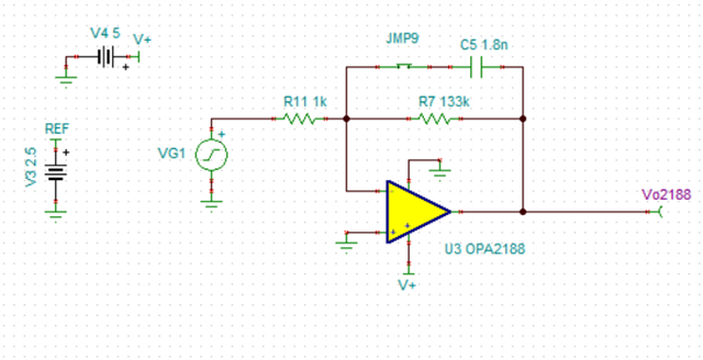
Config 2:
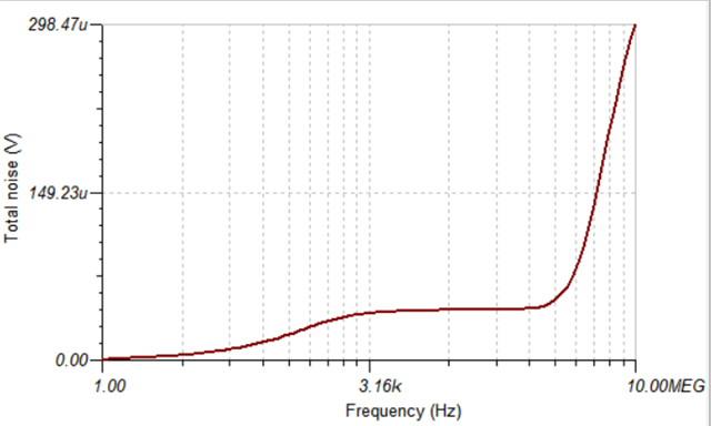
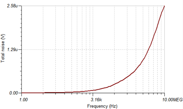
Here RMS noise shot up to 298uVrms.
1. I ran simulation till 10MEG, however if I increase the frequency, noise is still shooting up. Since the cutoff or BWn came around 1KHz, I have considered to run it till 10MEG. Any thumb rule for considering the maximum frequency based on BWn value?
2. I also noticed that if I reduce the REF voltage from 2.5, the total rms noise is reducing. However not able to correlate it to the calculation?
I made two changes, one added differential input configuration and second, added reference or dc offset to that. How do I correlate it in the calculation?
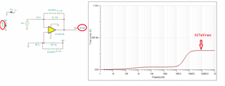
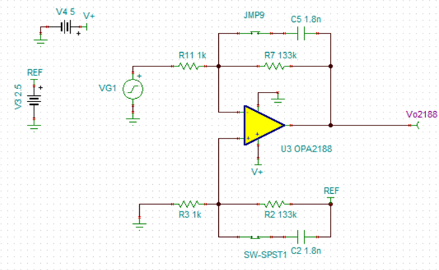
Config 3:
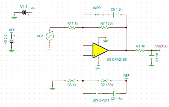
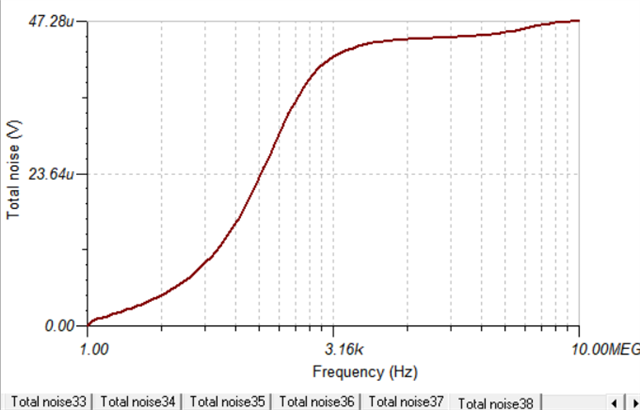
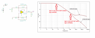
In this, external RC is added of cut off 159KHz and total rms noise reduced to 47.28uVrms.
Noise contributed by o/p RC stage would be:
e.n_r1k = √4.K.Tn.R = 4.05nV/√Hz
Since output RC has one pole, correction factor k = 1.57
BWn = k.Fc = 1.57 x 159kHz = ~250kHz
E.n = e.n_r1k * √BWn = 2.02uVrms
If above calculation is correct for external RC filter, how should I include it to achieve total rms noise = 47.28uVrms
Thanks in advance!
Regards,
Sunney