This thread has been locked.

If you have a related question, please click the "Ask a related question" button in the top right corner. The newly created question will be automatically linked to this question.

OPA860: OPA860 I_Q setting

Part Number: OPA860
Other Parts Discussed in Thread: DEM-OTA-SO-1A, TINA-TI

Hello,

I've expected to use operational transconductance amplifier (OTCA) OPA860 in my design as a wideband voltage to current converter (from a standard 50 Ohm equipment, and with output capacitance of 2+2=4 pF), and I've set it in a following schematic 

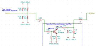
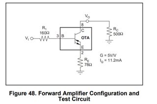
I did it as close as possible to typical application schematic in its data sheet (Figure 46, page 15):
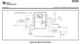
.

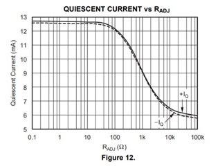
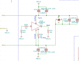
As it may be seen on the image from the device data sheet above, in order to make I_Q of OTCA to be about 11.2 mA, resistor Radj should be about 250 Ohm.

When I used 249 Ohm there I got V_Radj=37 mV --> I_Radj=148 uA --> I_Q=5.5 mA, which is below expected minimum of 7.9 mA, and I didn't found any signal current at the output.

I have had to decrease the Radj to 71 Ohm in order to start to see a weak signal current at the output. And in this condition the I_Q was still 6.77 mA, which is below the minimum value.

What is wrong with my circuit?

Thank you

  • Hello Pavel,

      I can't really see anything wrong with your circuit. With a low quiescent current,  the amplifier seems to not being powered on sufficiently. Can you double check the power supplies, and probe directly at the amplifier's pins Vs+ and Vs-?

    Thank you,
    Sima 

  • On package pins, at the point, where they enter plastic of the SOIC package (last metal):

    • pin 4 = -5.016V
    • pin 7 = 4.974V.

    They look normal.

    P/N OPA860ID, bought from Mouser on 24 Jul 2021. Date code: 08N8Z.

    It behaves the same way on two separate boards of the same layout.

    Rechecked the layout, it also seems to be OK.

    ???

  • Could you please, check with a product team about any issues with this date code?

    Thank you

  • Hello Pavel,

      Thanks for the additional information. We are looking into this date code with the quality team, and will update you with their response.

      Re-looking over this issue, the adjustment to pin 1 (Iq adjust) should only affect the OTA (transconductance portion of the device). The buffer section alone needs 5.5mA, the OTA would be the rest of the power consumption depending on the resistor selection at pin 1. 


      This could rather be an issue with the OTA rather than the buffer portion of the device. 

      Can you use this setup configuration for the OTA? You should get about 11.2mA of total quiescent current with the below circuit with Radj set to 250Ohms. 


    Thank you,
    Sima

  • Hello Sima,

    I do use only the OTA section of the device. A buffer is just terminated, see my schematic in the original question.

    I measure the OTA current consumption by measuring the voltage drop on R_Q itself, then I calculate a current through R_Q, and multiply it by 37, as it described in the data sheet. And get a current consumption of the OTA section only below the min value in the data sheet.

    For R_Q=249 I expect to get it about 11.2mA, but I got 6.77mA on two boards. This is the problem that I expect you to to resolve or explain.

    Thank you

  • Hello Pavel,

      I initially assumed that you were measuring the power consumption using the power supplies which would be connected to both the OTA and buffer, supplying current even if buffer is terminated.

      That is the correct way to determine the total quiescent current of the OPA860. Measure the voltage at pin 1 and subtract that value from -5V and divide by Radj, or measure the current with DMM at that connection. 

      Would it be possible to set up the OTA as done in Figure 48? That is the configuration used for the specifications in the device datasheet for the OTA section. The quiescent current specified in the datasheet (11.2mA) is under the power supply section for both OTA and buffer. There could be some confusion there; how much current is your power supplying?

    Thank you,

    Sima

  • Hello Sima,

    When I measured the OTA section's current I did what you described, I took a voltage drop on R_Q, calculated a current through pin 1, and multiplied it by 37, like it is described on the page 14 in the data sheet. And I got the result, which is below the min value in the data sheet. Please, see my original message.

    The OPA860 is a part of my design with many other circuits. They are all sitting on the same power rail, and I can't isolate this stage from others. If you want me to measure it separately, I can do it, but you have to send me the OPA860 evaluation board, where it will be the only active device. Then I will be able to measure it with any values of resistors. The tested device will be another component from the same batch.

    I would expect that you will do it on your side with a standard device, as a starting step.

    Let me know what you would decide.

    Thank you

    Pavel

  • Hi Pavel,

    What is the DC load impedance on the current output? Your schematic shows "Do Not Insert" for the R132 footprint, while the datasheet examples all have 500Ω for this resistor when using common-emitter gain. Is there too much resistance for the current to flow though? The 162Ω degeneration resistor is also more than double the 78Ω from the datasheet example. 

    Can you get an output current for a short from collector to ground, and if not, can you see any more current for a smaller degeneration resistor? 

    Best regards,

    Sean

  • Hello Sean,

    As I understand, the absence of the OTC output current in my case is addressed to the too low quiescent current of the OTC (see my original question),  which may be measured by measuring the current through R_Q (pin 1) and multiplying it by 37. 
    The load of the OTC section in my case is an input of the TIA (I use the OTC as an injector of the test signal), it has 2pF to ground and a very low input resistance, but again I am asking about the I_q, which as I understand should not be influenced by what load the OTC sees.

     The value of the degeneration resistors in emitter of 162 Ohm I took from the example circuit in the application section of the data sheet, and it works for me, so I’ve decided to use it. Do you think that it may influence the I_q of the OTC section?

     Thank you

     Pavel Margulis

  • Hi Pavel, I don't know that the Iq= 37 x I1 math holds up for a resistor load. That may only be true if you use a circuit like they have in Figure 45. Have you tried using 0 ohms for R_Q? That might get the output current up to what you need.

     It says that degeneration resistor should not effect quiescent current, but it will of course decrease output current.

  • Hello, Sean

    As I understand/guess, pin 1 is an input of the current mirror working with a ratio of 37, and this current mirror/s set a bias current of the OTC section combined. Would it take this current not from the positive power rail, but from the output, then the pin 1 current still should reflect it correctly and it should be as it is set, no matter where it comes from.

     As I wrote in my original message, when I used R_Q=71 Ohm, it started to operate somehow, but with pin 1 current (I_Q/37) still below the expected value for even lowest I_Q value in the data sheet.

    I didn’t try R_Q=0, simply since I didn’t want to harm the components. I can’t be sure about my guesses of how it is built inside.

     And we agree that degeneration resistors should not influence the quiescent current.

     To summarize - I think that neither R_E nor R_load should influence operation of pin 1 current. So, why it operates in that strange way?

     Can you send me the EVM of OPA860?

     Thank you

     Pavel Margulis

  • Hi Pavel, The datasheet says that there is 250Ω in series with pin 1 internally, so it should be safe to reduce R_Q further.

    As for the EVM, you will have to order one here for $5.  https://www.ti.com/product/OPA860#design-development 

  • Hello Sean,

    I bought, received and assembled OPA860 EVM DEM-OTA-SO-1A. Components that I installed are as following:

    • power: +-5V, 10uF and 0.1uF at both voltages
    • OPA860 is from the same batch as previous parts used
    • OTA section: RB2=51, RB1=150, RE=150, RC1=0, RC2=51
    • Buffer section: RBIN2=51, RBIN1=150, RBOUT1=0, RBOUR2=270, no connections at input and output
    • RQ1=250

    In terms of IQ it behaves in the exactly same way as the OTA on my board. V_RQ=35mV, IQ=37*35mV/250=5.24mA.

    Change RQ to 9.1 Ohm, increased the IQ to 7.32mA, but it doesn't influence the total g_m_deg, because it is governed by RE.

    I assume that the installed OPA860 and the EVM are OK, therefore, looking at these numbers and at Fig. 12 in the data sheet, I conclude that the IQ that data sheet relates on is a total IQ of the part, i.e. of OTA and Buffer sections together, (after reading the data sheet I thought that this is the IQ_OTA of the OTA section only) and that the Buffer section's IQ_B is about 6mA (remaining when pin 1 is practically disconnected according to Fig. 12 in the data sheet).

    Please, confirm this statement or correct.

    In case that this is correct, I have two conclusions:

    1. the OTA on my board works just fine
    2. the data sheet is complicated for understanding and misleading, because it has no definition of terms, like IQ

    I've measured the transfer function of the EVM with RQ=250. It is attached below. The measurement is done by spectrum analyzer SA44B and tracking generator TG44 from SignalHound. I expected that response will decrease with frequency, and it will have -3 dB at about 500 MHz, or at least 80 MHz as stated in data sheet.

    The transconductance, including the influence of RE, g_m_deg=1/(1/g_m+RE)=1/(1/0.125+150)=6.33 mA/V. Therefore total voltage gain is G=g_m_deg*25=0.158 V/V.

    I've expected to get 20*log10(0.158)=-16 dB. And I measured -15 dB at low frequencies.

    The absolute value at low frequencies is approximately correct.

    Now, two things that I still don't understand:

    1. a 0.5 dB rectangular deep in the frequency response between 15 MHz and 140 MHz
    2. why the gain is rising with frequency and not falling, is this real?

    Please, reproduce this measurement at your side and provide results and explanations.

    Thank you

    Pavel Margulis

  • Hello Pavel,

       Your statement is correct. The datasheet value is both the buffer and the OTA which is the total amount of current the power supply typically will sink/source into the device. 

       The frequency response suggests instability. To clarify, there are no connections to the buffer, so is this the open-loop frequency response of the OTA? Are you using SMA connectors, or are you probing the output? Due to the reason below:

    Thank you,

    Sima

  • Hello, Sima
    Confirm, buffer section is not connected, it has a 50 Ohm at its input and loaded by 270 Ohm.
    The graph is an Aol of the OTC section at (50 || 50) Ohm load (50 Ohm is installed on EVM, and another 50 Ohm is off the equipment through coaxial cable), with Rq=250 Ohm.
    I use SMA connectors, high quality coaxial cables, and of course it is measured in 50 Ohm system and with no other load. Please, reconstruct the test at your side and provide an explanation for seen effects.
    Thank you
  • Hello Pavel,

      Thank you for the additional information. The setup is correct, I am not too sure what other factors could be influencing it. I would suggest starting with original circuit used for characterizing the device (attached Tina-TI file below of the setup). If this setup works, we can fix from there and integrate your values. I will need to send in an order for device + board, since we do not have one currently available in the lab.

    OPA860_OTA.TSC

    Thank you,

    Sima