Other Parts Discussed in Thread: ALM2403-Q1
Hi team,
Customer get 2 questions on ALM2402F-Q1:
1. what's the rated current of output transistor's internal reverse diode?
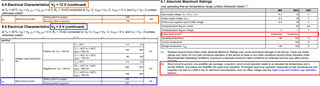
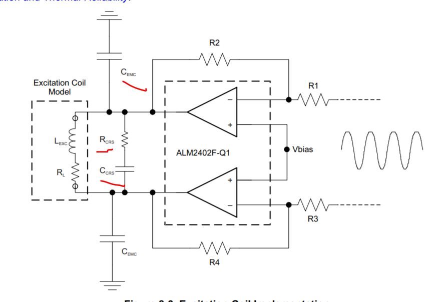
2. how to select the RC circuit of the output stage as shown below, please give some recommended value and select guide.
thanks!