Hi,
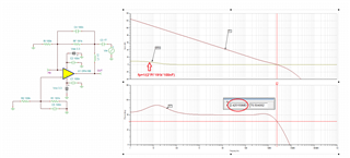
The below LPF is built using OPA4188, I have following questions
1. The pole in feedback because of input capacitance (Ccm, Cd, Cstray and Req = RF||Rin), causes the zero in 1/beta plot as show at ~130kHz, plots are shown below.
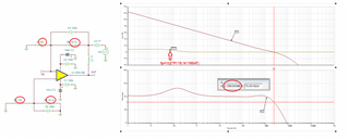
When CF is added to counter the pole in feedback path, zero is added at ~8.3kHz (second plot). It reduces the overall bandwidth of close loop to the placement of zero in the feedback path, is the interpretation correct?
2. When I scale down the resistor values to achieve same gain from RF 191k to 19.1k and Rin 100k to 10k, I receive similar results except pole in the feedback path will have different frequency ~1.3MHz. What other advantages I get if scale down the input and feedback resistor?
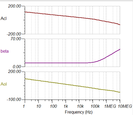
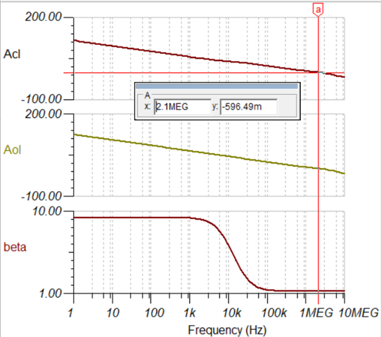
3. while doing the stability analysis (both the inputs are grounded), then why feedback path or gain is showing as of non inverting configuration?
Regards,
SunneyOPA4188_SIM.TSC