A related question is a question created from another question. When the related question is created, it will be automatically linked to the original question.
If you have a related question, please click the "Ask a related question" button in the top right corner. The newly created question will be automatically linked to this question.
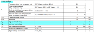
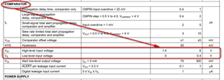
I have some doubts about the input range of the comparator: what do VIH and VIL refer to in the first screenshot below? How is it defined? Is it related to supply voltage VS? Shouldn't its input be analog voltage?
The VIH and VIL levels from the first shot dictate the voltage level that the device must see to register as a logic high or a logic low. This datasheet is specified this way to show that the value is independent of the supply voltage, but you are correct in the absolute maximum you show that the pin must not be exposed to greater than Vs+0.3V.
As an example, if you wanted to run the device with a supply of 3.3V, the pin would need between 0 and 0.4V to register a logic low, and would need to be driven to between 1.4 and 3.3V to express a logic high . Exposure to >3.6V on the pin would potentially damage the device.
If understand according to your idea, can't the two input pins of the comparator (CMPIN and CMPREF pins) input a voltage between 0.4V and 1.4V? If so, I don't think it's reasonable.
I suddenly had a bold guess whether there was a typing error here. Here should be the output high and low level range of the comparator. Is it possible?
This is not a typo, and is pretty common for many datasheets containing digital pins. The CMOS team covers this very question in an FAQ here.
The short answer is that the voltages between 0.4 and 1.4V are an undefined state. If the customer were to somehow provide a voltage of this range to the device, then the output of the comparator will be unknown.
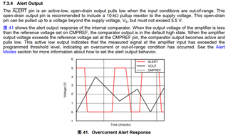
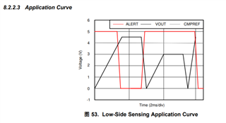
However, some pictures in the datasheet show that the CMPIN pin is directly connected to the VOUT pin, and the voltage range of the VOUT pin is 0V ~ 4V or 4V+. As shown in the screenshot below. If the voltages between 0.4 and 1.4V are an undefined state, it is also possible to output a low level (although the pictures in the datasheet output a high level), that is, ALERT pin outputs a low level. In this way, the overcurrent state cannot be detected correctly, because the ALERT output is uncertain when the voltage is 0.4 ~ 1.4V.
I understand the disconnect now. You are trying to apply these parameters to the comparator inputs, but these do not apply. These are defined logic states for the digital inputs pins, such as the reset pin. These do not apply to the comparator inputs.
However, these two parameters are under the column of COMPARATOR, which is easy to be misunderstood as the parameters of comparator. If it is not a parameter of the comparator, it is recommended not to put it under the column of comparator.
Understood, and I will relay this feedback to the team. We place this information underneath the comparator section because the reset pin is a portion of the comparator section of the IC, controlling whether the device operates in transparent/latch mode.