This thread has been locked.

If you have a related question, please click the "Ask a related question" button in the top right corner. The newly created question will be automatically linked to this question.

INA118: INA118 for EEG (anyone with any INA experience welcome).

Part Number: INA118
Other Parts Discussed in Thread: INA826, INA826EVM, INA818

Hi,

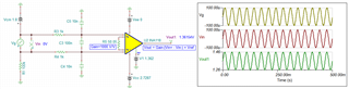
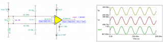
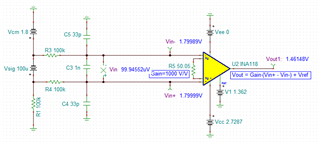
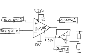
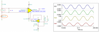
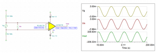
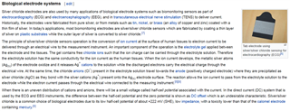
I am currently designing a basic EEG circuit, i have centered the design around the INA118, the design is shown below.

I have followed the general/classic architechture. Instrumentation amplifier, single supply (battery powered, LDO regulated), buffered midrail used for REF pin, common mode noise extracted from gain resistor(s), fed into unity gain buffer, inverted and fed back to right-leg drive electrode.

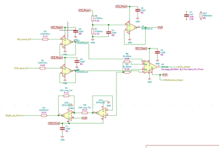
I have also buffered the input signals from the electrodes as I intend to use dry electrodes (design constraint). Picked up the buffering idea from a TI resource, supposed to help reduce DC offset that comes with using poorly balanced dry electrodes.

The problem:

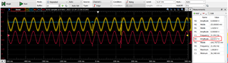
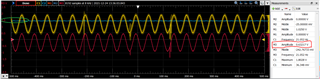
Right now, the whole thing feels like a complete non starter. Every signal generator signal i put into the inputs, with or without the input buffers, returns inconsistent rubbish!

I cannot actually use the circuit with EEG pads, on my head, as there seem to be so many variables that every time i think i am getting somewhere, i discover something that is stuffing my results (my foot being near a plug socket, my laptop charger throwing off noise, the fact i've built it on vero-board - which is touching my jumper - magically coupling it to my stereo)... one of those hair pulling circuits. Yes the driven right leg solves a lot of these issues, but that assumes i'm attaching it to my head, which is a run-before-you-walk approach and doesn't produce consistent enough results. Only a few times have i seen an output signal even close to what i'm after.

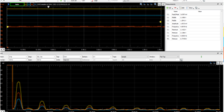
I'm using an AD2 analogue discovery with BNC adapter for high impedance probes as a signal generator and a scope, which frankly, i'm not all that confident in the integrity of (feel free to comment). I prefer the picoscopes, but currently dont have one. Or better still, any average bench scope.

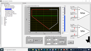
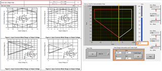
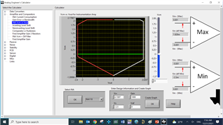
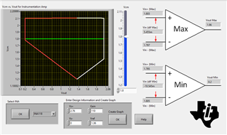
I downloaded the Ti Analogue engineers calculator tool to try and better understand the input constraints of the circuit see below:

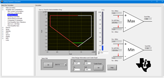
Am i right in thinking the CM voltage shown on this calculator refers to the DC offset of the input signals (when attaching a sig gen to the inputs, i've simply increased the offset voltage of the signal)?

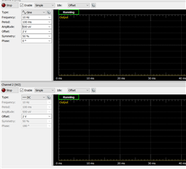
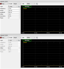
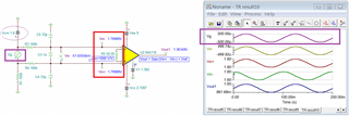
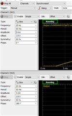
Currently i'm inputing the VCM as a 1.3V DC signal into the inverting input. and a sine wave ~10Hz, ~100uV amplitude, 1.3V offset into the non-inverting input (my pretend EEG). With both reference clips on 0V.

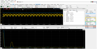
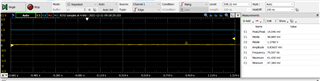
What i'm seeing is usually a tiny noisy looking squarish wave with a gain of ~no-where-near-enough. I have, in the past, seen the desired gain of 1000, but usually with higher input amplitude. This gain then changes MASSIVELY with chages to the input offset (or VCM?)

All i want to acheive: Is to input a couple of signals vaguely similar to EEG signals (50-100uV amplitude, this is the lowest the AD2 goes) and see those signals, appear at the output with the 1000gain applied.

My ultimate goal here being of course to identify some of my own alpha waves and consistently influence them with the classic eyes open/eyes closed experiement.

If someone could suggest an exact physical placement for sig-gen probes, reference clips, scope probes & reference clips, feel free. Feel i'm not actually getting the input setup correct?

On the EEG front, do i assume that the DRL electrode will suitably increase the potential of my body with reference to 0V, so as to acheive the VCM required for the INA;s input?

I appreciate some of the above is a bit garbled and may lack in information. I'm trying to avoid this becoming a really long post, don't want to deter folk. This is really simple stuff and shouldn't be this hard, honestly, any general comments from other INA users, EEG/ECG/EKG folk, would help.

Many thanks,

Sean

  • Hi Sean,

    Enclosed are series of videos about ECG measurement requirements. There are 6 video series that you may be interested. 

    https://training.ti.com/how-measure-ecg-introduction-what-ecg?context=1128637-1128609

    Enclosed is an example of INA118 with Gains of 1000V/V. If you are able to provide me with more configuration details in EEG, we may provide you with a simulation for the application. The LPF filter in the circuit below is not quite correct, since your application is required to reject the common mode noise above 50/60Hz range. Once I have more details, we can build the simulation on top of the basic circuit including simulating the dry and reference electrodes etc. in the application. It will be good if you are able to provide us these pspice models.  

    INA118 EEG-1 12202021.TSC

    Below is the Vcm vs. Vout configuration from the data you provided, where the input Vcm voltage is configured at approx. 1.8Vdc. 

    Please also take a look at INA826, where Figure 69 is shown an ECG Circuit and example. 

    https://www.ti.com/lit/ds/symlink/ina826.pdf?ts=1639998529029&ref_url=https%253A%252F%252Fwww.ti.com%252Fproduct%252FINA826%253Fqgpn%253Dina826

    If you have additional questions, please let us know. 

    Best,

    Raymond

  • Hi Raymond,

    Thanks a lot for the reply & taking the time to read my post!
    I'll take a look through the videos, i think i've seen some of the TI EEG/ECG vids, but some of those are definitely new to me.

    Unfortunately I would say i'm not quite at the "actual EEG" stage yet, as i previously eluded to, i'm still waiting to see success with a signal generator before trying to make sense of brain waves. I dont have access to anything in the realms of pspice & really i just want to get the chip working in a VERY basic sense, & understand what i am doing wrong first.

    The "shared" cap on your INA118 example, (vertical between the inputs to the INA), i've seen this in the past but i am not certain of it's purposes? Of course i can see the 2 LPF's, just not sure where that 3rd cap fits in?

    I should add context and note that my output signals are being sampled by an ADC at a reasonably slow rate (~256Hz), and then run through FIR filters to isolate the alpha and theta bands. Hence why no passive filtering was included on the initial schematic (not that it wouldn't hurt).

    The figure on the INA826 datasheet was actually one of the first EEG schematics i ever found when i started the project & was probably what led me to using the INA series, so good to know i'm hopefully at least on the right tracks.

    To try provide more detail as to my problem:

    As you saw, i did use the TI calculator to come up with input characteristics to you, I think what i'm trying to understand is more about the input conditions and how i can emulate these.

    My issue is that i dont fully understand the need for the VCM voltage and how to experimentally input this voltage. Also when using the EEG circuit in situe (on head, not sig gen), how are the EEG signals from my head, biased to VCM?

    Currently, I have 2 sig gen channels, each generator is attached to an input of the INA (as mentioned in original post), these are setup as below:

    Is my use of the offset voltage on the sine wave, and the DC voltage (no sine wave) an appropriate way to input the VCM to the circuit? The 10Hz signal is meant to simulate a differential signal, comparable to alpha waves.

    The above input parameters, result in the below output. Yellow trace is out pin, Blue is ref pin.

    Note that the amplitude of this wave is not consistent with a gain of 1000 (yes, i have some 0.1% tolerance resistors on the gain pins, so we should be ok there).

    Also i cannot seem to get any output with my VCM much below 2V (let alone 1.8V): Below, all i've changed is the DC offset, from 2V, to 1.8V and i've gone from an over amplified wave, to a flat line.

    Why is the output wave in my working example (2V VCM), not centered around Vref?

    I also seem to contantly be able to push the chip past the parameters produced by the TI calculator, (for example, the calculator suggests for 2V VCM Vout minimum should be 0.2V, but if i keep increasing the input amplitude to push the output harder, the trough of the output wave goes most of the way to 0V!)

    I'm sure my issue is connected to how i've produced the VCM in my input signals, or the way i've physically connected up the scope & sig gen. I've removed my input buffer chip and i am not pretty much down to just the INA118 on the board and a buffer for the ref voltage. So there is very little left to go wrong by way of components or design.

    Key question here is, is my sig gen setup the correct way to acheive the desired VCM?

    Thanks again,

    Sean

  • Hi Sean,

    Let us talk about the relationship of the input common-mode input voltage vs. Vout. Vcm is defined as an input voltage range in which the op-amp's output will respond linearly when the input is applied to the op amp's  Vin+ and Vin- terminals. For INA118 instrumentation amplifier, these specification are listed in the datasheet as captured in the image below. The instrumentation output voltage transfer function is described as: Vout = Gains* (Vin+ - Vin-) + Vref, when it is operating linearly, and (Vin+ - Vin-) is the differential input voltage at the input pins of INA118. As in your case, the differential input voltage is approx. from 50uV to 500uV range.

    With EEG's input signal from 50uV to 500uV range and Gains = 1000V.V per your low input voltage supply rail, it is good to place the input Vcm at approx. 1.8Vdc, which it can maximize the input voltage ranges and the output voltage swing, as shown in the simulation below.  

    In the captured simulation below, I simulated an example, say an EEG's differential signal is 100uV, Vcm = 1.8V and Vout = Gains* (Vin+ - Vin-) + Vref = 1000*99.94552uV + 1.362 = 1.461945 V. The simulation has a slightly different figure, since my hand calculation did not take into account of INA118's offset voltages when Vsin = ± 0.000x mV. 

    Here is how Vcm may be configured in simulation: Both Vin+ and Vin- has an input common mode voltage of approx. 1.8Vdc, and Vg (the signal generator) has differential input voltage swing from -500uV to +500uV, and Vout1 is the simulated output voltage from INA118.  

    If you do not want to apply the bias voltage on a patient's head, you have to use dual supply voltage rails as shown below. 

    Regarding how to configure common and differential mode LPFs in front of instrumentation amplifier, please see the INA826EVM application note.  

    https://www.ti.com/lit/ug/sbou115c/sbou115c.pdf?ts=1640099522391&ref_url=https%253A%252F%252Fwww.google.com%252F

    If you have additional questions, please let us know. 

    Best,

    Raymond

  • Hi Raymond,

    Thanks again for the reply and putting the simulations together.

    I understand the signals i should be inputting according to your simulations etc and the relationship between Vout & VCM, but my question in not about simulated inputs, as i previously eluded to, my doubts are in the experimental implementation of the circuit.

    I've repeated the experiments but with slightly more concise input signals:

    As before, I have 2 sig gen probes attached, one to each input, now with 2 sinusoidal signals, fully out of phase.

    1.8V common mode voltage present, i've lowered the amplitude to ensure the differential component to the input is well within the operating range provided by the analog engineers calculator tool.

    But still the ouptut does not exhibit anywhere near enough gain. (red math channel is Vout-Vref)

    Currently, my setup contains ONLY, the INA, the buffered reference supply, the gain resistor & a decoupling cap on the INA power supply. No input filters, only the signal generators, attached straight to the INA inputs.

    As best as i can see, the conditions i have put into the chip, exactly reflect the conditions from your simulations and the results provided by the calculator tool (bar the amplitude of the differential signal, i've tried many amplitudes here). The only thing that seems to provide even close to sensible results, is increasing the common mode voltage to ~2V, anything below ~1.95V and the output diminishes massively. Yet the gain of the chip is still not consistent with the calculations. So my question is, not regarding the theoretical implementation, it is the experimental implementation that is causing problems.

    I mentioned previously, could you please let me know the purpose of the cap in parallel with the INA inputs?

    Thanks again,

    Sean

  • Hi Sean,

    Jumping in here since Raymond may be on holiday.

    These three capacitors are called common-mode and differential mode capacitors. The two capacitors to ground are the common-mode capacitors and those filter out common-mode EMI signals, whereas the single capacitor between the two inputs remove EMI that appears as a differential signal. 

    The resistors you see at the inputs combine with these capacitors to form a first-order low pass filter roll-off (-20dB/dec). However, the -3dB cutoff frequency is different for the two modes. The differential cutoff frequency must be set such that the desired signals are not attenuated. For example if the maximum differential signal frequency is less than 100Hz, a -3dB cutoff of about 350Hz will be required to avoid excessive attenuation at 100Hz. The resistor values should be kept small to keep the resistor noise contribution low. The smaller the resistor value is made the larger the filter capacitor values become for a given cutoff frequency. So a compromise is called for.

    The usual practice is to set each common-mode capacitor,  to 1/10th that of the differential-mode capacitor. The reason for doing so is to reduce the filter’s ability to convert the common-mode signal to a differential signal due to common-mode capacitor mismatch.

    In your experiment, are you using the INA118? We expect your circuit to work as we simulate. We may consider trying a different INA118 chip, or even swapping it out for a modern solution like the INA818. 

  • Hi Tamara,

    Thank you for explaining the use of the caps, i've seen various configurations across several reference designs & rarely an explanation of their purpose. So that helps a great deal.

    I'd like to stick to the traditional INA series of 2 & 3 amp instrumentation amps, to try and maintain some portability, i've had some recent issues with suddenly discontinued components from TI & of course the silicon shortage. So the more versatile i can keep the circuit, the better.

    I've now stripped the circuit back, i've actually reverted to breadboard, as my veroboard was becoming a mess. 

    I have come to the conclusion the Analogue Discovery 2, that i was using performs pretty poorly in the micro volt regions. So i've reduced the circuit gain to ~110, to allow me to use larger input amplitudes.

    I've revised the circuit with the view to simplfying it and removing any potentially suspect components or other unknown variables, I know without the filters etc, i wont see optimum performance, but currently, i want to see this chip actually work (yes i've tried swapping a fresh chip in & perio, then i'll think about filters etc. Excuse the poor quality, using a tablet is much quicker than KiCAD, but i'm not all that good with the tablet...apparently: (This really is, all i have on the breadboard, NOTHING else)


    I've recalculated the Vout Vs VCM profile for the new gain resistor.

    See below the sig gen signals, where Vdiff = V1-V2/2 = ((1V+3mVSIN(wt))-(1V-3mVSIN(wt)))/2 = 3mVSIN(wt) amplitude... in theory,

    and the subsequent output:

    With a fully differential signal, i should be seeing the previously calculated differential amplitude * gain = 330mV (gain is now ~110), yet as you can see there is an amplitude of more like 630mV.

    Sure, there will be a DC offset no doubt & there are a number of aforementioned inaccuracies in the probes & sig gens (i have trimmed the probes and run the signal generators straight into the scope, to make sure they are producing sensible signals, and they are....to within a few %, so i would expect a little of the differential voltage to be "seen" as common mode & vice versa)

    But nowhere near enough to result in the output amplitude being nearly double the expected value, i have a feeling perhaps the equation i've used above for differential mode voltage here is for average differential mode, not necessarily the voltage i would see from the output of the INA? In which case, the output is actually ok.

    As far as i can see, my input signals are within the max & min ranges specified by the calculator (second screenshot).

    Can you confirm my input signals are within the parameters set out by the calculator?

    Have i calculated the differential mode votlage correctly? - seems convenient that the output would be roughly double the intended output... have i missed a factor of 2 somewhere?

    We expect your circuit to work as we simulate.

    Definitely some irony in this statement, ha.

    Thanks again,

    Sean

  • Hi Sean,

    I have not totally read all the posts of this thread. But me thinks that the "right leg" stuff is something more suited for ECG instead of EEG.

    What you need is a ground electrode. If you have three electrodes on your head, connect one of them to signal ground of your circuit and the two others to the two inputs of an instrumentation amplifier. And remove all this "right leg" circuitry for a moment.

    Also, to ease things, power your circuit with a bipolar supply voltage, like +/-1.5V or so. Better you take OPAmps allowing a higher supply voltage like +/-9V. The use of a bipolar supply voltage gives you a true and low lohmic signal ground, much better than when using a single supply voltage.

    More, don't play with your health. Only take batteries to power your circuit!!! And don't increase the battery voltage to more than +/-9V!!! And: To connect your EEG circuit to other electronics, a safe galvanic isolation is needed!!!

    Don't electrocute yourself, it's Christmas day :-)

    Kai

  • Hi Sean and Kai, 

    Thanks for Kai's reply and greetings! Welcome back and Happy Christmas!

    I saw your signal generator's input signal, but I am not clear how it is applied to the INA118's differential input. Please annotate the screen shot. 

    What is Turquoise color, which is centered approx. at 1.4V or so?

    Based on yellow line, it may be the output, but it is centered at (1.8V -0.5)/2 = 0.65Vdc. Where do you captured the red line, which is centered approx. -0.15Vdc. Please draw out your input schematic by hand, if you do not have it in drawing. 

    If you apply the signal input signal, say ±3mV, 20Hz on top of Vcm = 1.8Vdc, below is the current simulation. Yes, the INA118's simulation should match the

    actual physical setup on PCB or breadboard. 

    INA118 EEG-1 12242021.TSC


    If you are using +/-1.5V dual supply rails (e.g. two dry cell AA batteries), you do not have to concern about the Vcm as much, see the attached simulation (as suggested by Kai).  

    INA118 EEG-3 12242021.TSC

    The image below is captured from the internet site below. You may consider to use solid state Ag/Ag/Cl reference electrode for an EEG electrode reference . I am not expert of the EEG application, but I think that the ionic/electrical interfaces to human head/skin surface in biological application may be more stable, consistent or repeatable measurement than a simple reference ground. You may read about the Pros and Cons of the EEG application.  

    https://en.wikipedia.org/wiki/Silver_chloride_electrode

    Best,

    Raymond