This thread has been locked.

If you have a related question, please click the "Ask a related question" button in the top right corner. The newly created question will be automatically linked to this question.

INA293: Output voltage overshoot while evaluating with current step response

Part Number: INA293
Other Parts Discussed in Thread: INA240

Dear experts,

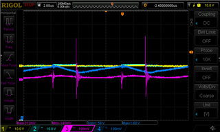
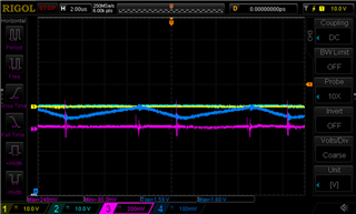
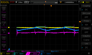
could you please help me find out what could be the root cause for significant output voltage overshoot as seen on oscillograms below? Target application is INA293B3 (100x  gain), low side sensing, 0.5mOhm shunt, 60A.

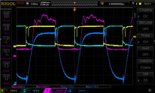
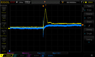
Yellow: INA output (500mV/A); blue is external current sensor (25mV/A; 1.5MHz). Step change of load from 0A to 0.5A, low side sensing, resistive load, shunt 5mOhm.


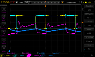
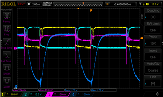
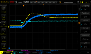
Yellow: INA output; dark blue is external current sensor (25mV/A), light blue is DBbus voltage. Step change of loadfrom 0.5A to 5.2A, high side sensing, resistive load, shunt 5mOhm.

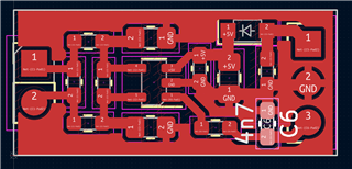
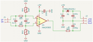
Schematic is below. 50R on negative input is to provide 100mV offset. Visible on first oscillogram.

I have tried to remove input filter, replace INA, place 10KOhm resistive load to output, remove C6 capacitor or place 4n7. Nothing helped. and I have run out of ideas.

Thanks for support

Stanislav

  • Hello Stanislav,

    Can you confirm if there is a transient VCM voltage due to current switching and parasitic inductance.  If this is the case you may be seeing some AC CMRR issue.

    I have done step responses before with this device and I have not seen anything like this.  I see you avoided the low saturation by placing an offset on the device but other than VCM transient changes I do not see what the issue could be.

    If you would like I can attempt these same scope shots with one of our EVM to compare but I think it is more likely due to parasitic when switching.  Another thing to check is make sure the GND node is solid and does not change as well.

  • Hi Stanislav,

    I aggree with Javier, this noise is often the consequence of a poor grounding management. Can you show your layout and a scheme showing your ground routing?

    Can you show a scope plot of common mode input voltages from pin 4 to pin 2 and pin 5 to pin 2 of INA293? And connect the ground pin of scope probe directly to pin 2 by using such a ground spring:

    Kai

  • Hello Javier and Kai,

    thanks for your quick response. Thanks for pushing me to right direction. I just underestimated the difficulty of current sensing across the shunt. Typical "how hard can it be" situation. Slight smile

    Im trying to evaluate INA293B3 feasibility for existing inverter design so it is assembled on small PCB. The oscillograms above were caputred with this prototype PCB attached  via 30cm wires (both load and supply) floating on the bench. So for sure that caused the issue and therefore I mounted the INA board directly into inverter PCB (wires to shunt are below 2cm and wires to supply and MCU approx 4cm).

    Now it seems much better but there are at least few points to solve. See below.

    Yellow: phase A; lblue: phase B; pink INA out (from phase B shunt 0.5mOhm, should measure when light blue is low, low side sensing); dark blue is external current probe (25mV/A). Voltage 22V and resistive load 22Ohm -> dark blue curve shows 20A peak to peak and should have same scale (4A/div). Measurement taken with oscilloscope probe with GND spring as shown.

    Issue 1) Rising edge of INA output is often overshooting.. in general unstable. I believe it is caused by ringing across the shunt. I originally thought I will remove it by differential filter but I had to get rid of it in order to solve output saturation when current is zero. Could you propose any input filter which would also prevent low saturation?

    Issue 2) I think this 50Ohm resistor in IN- seems to create gain error. In datasheet it is evaluated for symetric input filter. Could you please help me to evaluate this error for asymetric input filter (like 10R in series with IN+ and 50R in series with IN-)?

    This is same measurement as above, but load resistor 22R is in series with 47uH inductor. Initial overshoot is visible... what concerns me is that INA output is quite below 100mV initial offset created by 50R in series with IN-. This wasnt the issue with purely resistive load...

    BTW parallel issue for me to solve is to reduce shunt ringing.

    Pink is measurement across shunt with probe with spring GND. (22R in series with 47uH load).

    Same measurement with only 22R resistive load.

    Oscillogram between INA GND and IN- with GND spring probe as requested (pink line)

    Oscillogram between INA GND and IN+ with GND spring probe as requested (pink line)

    Thank you very much for support.

  • Hi Stanislav,

    input filtering is a major cause of problems in combination with current sense amplifiers, because they tend to destroy the balance between the two inputs and result in a massive degradation of common mode rejection.

    That's why TI doesn't recommend input filtering. They merely worse things.

    So just omit all input filtering components for a moment. Have the shunt directly (!!!) mounted at the input pins of INA293. Do not have any cabling between the shunt and the input pins of INA293. This would add uneven parasitic common mode impedances which will totally ruin the superb common mode rejection of INA293. Also see section 10.2 of datasheet.

    Kai

  • Hello Stanislav,

    You could also look into using the INA240 which is meant to deal with larger Common mode spikes.  You could also add a reference voltage to either be bidirectional or move away from the rail to decrease the chance of saturation.

  • Dear Kai, Javier,

    thank you both for support and sharing experience. It certainly is a big know-how to measure current across low value shunt resistor at 100kHz switching frequency. I haven't fully solved the issue but at least the prototype of inverter works for current development cycle and I (probably) fully understand the issue. Major root cause being ringing of shunt resistor 0.5mR as you pointed out immediately (due to its parasitic inductance 0.5nH - 2nH as specified in datasheet).

    I ended up with asymmetric input filter 10R IN+; 330R IN-; 2n2 differential capacitor which gives me 640mV of offset (to prevent output low saturation due to ringing) and also has cutoff frequency 213kHz. Also the behavior of INA got much better when I reduced shunt ringing frequency and amplitude significantly with usage of "high side drain to low side source 3u3 capacitor".

    I understand that there are multiple issues with setup above so I will just briefly evaluate it and for next development cycle I will most likely look for another device.

    Thanks again and wish you nice day!

    Stanislav