This thread has been locked.

If you have a related question, please click the "Ask a related question" button in the top right corner. The newly created question will be automatically linked to this question.

PGA117: mux switch frequency of PGA117

Part Number: PGA117
Other Parts Discussed in Thread: OPA365, OPA320, OPA325, TMUX1308, OPA348, OPA392, OPA377, OPA3S328, OPA2325, OPA4325, TMUX1309, OPA328, TMUX1108, TMUX1109, ADS131E08

Hello

I would like to know the application of PGA117.

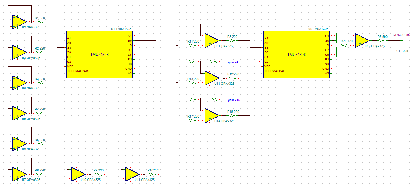
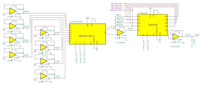
I have a six channel input signal, which is 50Hz. And I would like to use an ADC to sample all of them.

Can I use PGA117 for channel and gain selection?

The gain selection will not switch a lot, I have a determined value after power on.

But the channel selection is quite frequent, I want to measure all the six channels. The current signal is 50Hz.

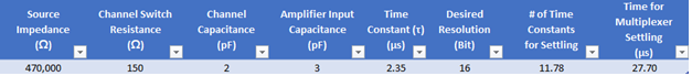
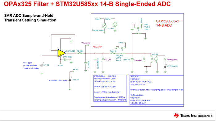
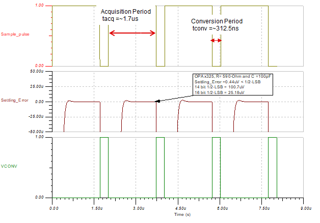
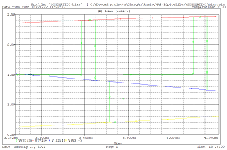
And for each channel, I will stay 64us for sampling, then to another channel. The sample-hold time is 1.7us, means I have 1.7us to charge the CSH capacitor.

Is PGA117 suitable for this kind of application, is the mux of PGA intend to use for high frequency?

Even all the six channel are all 50Hz, the signal level difference between each channel could be high.

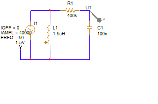
Could you help provide a simulation?

  • Hi,

    section 8.5 of datasheet shows the settling time. Seems that the settling time of PGA117 is at least 2µs. Would this fit?

    Kai

  • Hello,

    The PGA117 can certainly be used to measure 50-Hz signals.  Depending on the resolution requirements of your application, and the source impedance of the sensor or circuit driving the multiplexer, it may meet your settling requirements. 

    Regarding the multiplexer channel settling, the PGA117 datasheet offers Table 1, 'Frequency Response versus Gain'.  The datasheet provides the expected settling time vs gain with a 100pF +10k capacitive load.  The settling time with gain 200-V/V for an output 4Vpp signal to 0.01% is 10µs. 

    In your application, provided that the source impedance of the circuit/sensor driving the multiplexer is not too high, and depending on the target ADC resolution, the multiplexer should settle in the 68µs that you are allowing per channel.  Settling to 0.01% corresponds to about ½ of LSB (least significant bit) of 12-Bit resolution.  When driving the ADC, the datasheet recommends using an R-C kickback filter of 100-Ohms and 1nF between the PGA117 and ADC for optimal performance.  The RC filter will slow the settling slightly but you should still able to settle within 68-µs to 0.01% resolution.

    Regarding the sampling / acquisition time that can be supported, the device is able to drive the sample-and-hold and settle to 12-bit resolution of approximately 2µs when driving an RC filter of R=100Ω and C=1nF.

    - What is the ADC bit resolution requirement, and the sample-and hold capacitor value?  Which ADC device are you driving?  Since you are allowing 68-us per channel, is it possible to extend the sample-an-hold sampling time from 1.67µs to 2µs?

    - What is the output impedance of the sensor or circuit driving the PGA117 multiplexer inputs? (Or what circuit or sensor is driving the PGA117 mux inputs?)

    Unfortunately, this device was developed over 12-years ago, and there is no detailed simulation or official TI SPICE model available, but we may be able to provide calculations or approximations.

    Thank you and Regards,

    Luis

  • Hi User,

    what ADC are you intending to use?

    Kai

  • HI User,

    Please provide the details of the ADC part number, the ADC bit resolution, and the sample-and-hold capacitor value (if available).  Also, let me know if you have the flexibility to adjust or extend the sampling time; since you allow 68us for multiplexer settling.  

    The PGA117 datasheet mentions the device can support sampling at 500-kHz for 12-bit resolution SAR ADC but it is not explicit about the acquisition time and conversion time of the specific ADC; however, we may be able to provide an estimate of sampling time supported.

    Please also let me know the details of the circuit driving the PGA117 or the output impedance of the circuit that is driving the mux of the PGA117.

    Thank you and Regards,

    Luis

  • Hi User,

    another option is to insert a specialized ADC buffer between the PGA117 and your ADC, like the OPA365, for instance. Its 0.01% settling time is only 300ns Relaxed

    Kai

  • Hello Luis

    The ADC is a Micro embedded ADC, which is STM32U585. It is 14 bit, and we may use 16 times over-sampling, so for each conversion cycle, it is 4us in most. The Csh is 5pf. The output impedance of the circuit is 470kohm, it is not low output impedance circuit.

  • Hello

    In this application, the output of the PGA make me feel very strange, it is the combination of 3 50Hz sine wave. And the signal changes every 64us. I wonder is it a normal use? And in some case, I handle the 3 signal indepently, use the micro embedded mux to switch channel. Seems this is more normal and what people use to do

  • Hi user,

    please show some scope plots.

    You have 6 input channels and switch 15625 times per second between them? And each channel is switched to the output of PGA117 for a period of 64µs? And then you want take one sample in this 64µs period?

    Kai

  • Hi User,

    Multiplexer Settling

    The multiplexer (without accounting for the internal PGA117 amplifier settling) takes approximately 27.70-µs to settle within ½-LSB of 16-bit resolution when driven by a 470kΩ source.

    If the source impedance is 470kΩ, the settling of the circuit is dominated by the interaction of the source impedance with the channel capacitance of the PGA117 multiplexer and the internal PGA117 amplifier input capacitance.  In order for the multiplexer to settle within 16-bit resolution, after a full-scale channel change, you will need to wait a delay to allow the multiplexer to settle:

    TMUX_Settling = τ * (N + 1) * ln (2)

    Where N is the desired bit resolution (N =16-Bit) and τ is the time constant that forms with the interaction of the source impedance and the input capacitance(s) of the circuit:

    τ = ~ (RSource + RSW) * (CCH+ CAMP)

    Approximate calculation of Multiplexer Settling:

    This multiplexer settling calculation does not account for the PGA117 internal amplifier settling.  However, given that Table-1 of the PGA117 datasheet shows that the PGA117 will settle to 0.01% resolution (or ½-LSB of 12-Bit resolution) in 10µs at G=128V/V after a 4Vpp output step change; a 68-µs delay is enough time for both the multiplexer and PGA117 circuit to settle within 16-bit resolution after a channel change.

    ADC Sample-and-hold Settling

    There is no official PGA117 SPICE macro that accurately models the output impedance over frequency to simulate the settling or driving of the sample-and-hold and unfortunately the output impedance characteristic is not provided on the PGA117 datasheet. However, the circuit of Figure 75 shows that the device can support 16-Bit settling at 300-kHz while using an RC filter of RFLT= 100Ω and CFLT = 1nF between the PGA117 output and ADC input, while driving a 40-pF sample-and-hold.  The datasheet is not explicit as to how much of this conversion cycle is acquisition time and conversion time; however, if we make a conservative assumption and allow 1/300kHz = 3.33µs for acquisition/sampling time to charge the Csh=5-pF sample-and-hold, the device will settle easily.

    Are you allow to program the STM32U585 for an acquisition time to 3.33µs? It sounds like your conversion cycle time is 4µs.  Let me know if you will require a more detailed analysis, creating a simplified model incorporating the slew rate and small -signal gain and output impedance over frequency may be possible but will take time.  Alternatively, if you will require a much shorter acquisition/sampling time you could consider buffering the device.  The OPA325 (10-MHz) or OPA320 (20-MHz) could be considered to buffer the PGA117 in this application.

    Thank you and Regards,

    Luis

  • Hello Luis

    Thanks for your detail explanation. It is really helpful. How about use TMUX1308 & opa348, the gain is 12 times. How to calculate the settling time. The ADC sample hold time is 68 cycles, the clock is 40MHz, so it is 1.7us. And the conversion time is 12.5 cycles.

    Could you support on the TMUX1308 + opa348 settling time calculation?

    Thanks!

  • Hi User,

    the OPA348 shows a settling time of 7µs which is way too high for your application. Why not taking the OPAmps Luis and I suggested to you, namely the OPA320, OPA325 or OPA365?

    Kai

  • Hi User,

    The OPA348 is a 1-MHz bandwidth op-amp optimal for low-power applications.  This device will not support a sampling period of 1.7µs to charge the sample-and-hold due to its higher output impedance.

    A rail-to-rail input/output amplifier with higher bandwidth and a lower output impedance over frequency will be optimal to drive the ADC.  Choose an amplifier such as the OPAx325 (10-MHz) and OPAx320 (20-MHz) that are often used to drive ADCs. The OPA392 (10-MHz) and perhaps the OPA377 (5-MHz) are also a possibility for this application.

    Since the mux is driven with a high source impedance of 470kΩ, you have to carefully consider the interaction of the source impedance, and total parasitic capacitance of each channel. The PGA117multiplexer offers relative low capacitance of about 2pF typical, and the PGA117 internal input amplifier has a input capacitance of ~3pF, and therefore is typically able to settle within 27µs to 16-bit resolution as estimated on the previous post. 

    Discrete multiplexers bond out the output pin, and may exhibit larger channel capacitances. Most discrete 8:1 multiplexers offer CON channel capacitances in the ~10pF to ~20pF range.  Discrete op-amps inputs will also present input capacitances in the range of ~10pF.  When you add the parasitic capacitance of the PCB board to the total capacitance, and calculate the multiplexer settling time, this yields to channel-to-channel settling times around ~110µs to ~250µs range when driving the circuit with a high 470kΩ source impedance. 

    It is possible to use the OPAx320 or OPAx325 on gain 12x configuration driving the ADC; but the challenge becomes to reduce the 470kΩ source impedance or buffer the 8 multiplexer inputs which will add cost and area to the design.

    As mentioned by Kai above, a good solution providing good precision/accuracy, and a reasonable compromise in the settling performance will be to use the PGA117 in the selected gain configuration, and then buffer the PGA117 output with the OPAx325 configured on G=1. This will meet your 1.6µs sampling requirement and may offer a reasonable channel-to-channel settling time.

    I am working on a TINA simulation and will provide an update with the STM32U585 ADC and op-amp buffer within the next few hours.

    Thank you and Regards,

    Luis

  • Thanks Luis

    OPA348 is just an example. You may change to whatever amplifier you think possible. For me, an important thing is to get the spec(requirement) of the Amp. So let's forget OPA348

  • Hi User,

    In this application, the output of the PGA make me feel very strange, it is the combination of 3 50Hz sine wave.

    Please give us a scope plot which shows the three sine waves at the output of PGA117.

    Kai

  • Hi Kai

    Sure. The signal is a combination of 3 sine wave. For each time slot, it is 512us. For the 1st 64us, it is the shape for L1, for the 2nd 64us, it is the shape for L2, and for 3rd 64us, it is the shape for L3. And for the rest 320us. No signal. Prepare for some other channel.

    file 1 is the original 3 channels signal. file 2, the green curve is what I want to combine the 3 channel signal. file 3 and file 4 is the detail of the signal. You may see in file 4. The green signal first follow the blue signal, then yellow, then violet. Due to the combination of the TMUX, there is some overshoot and overdamp.

    2476.pdf2.pdf3.pdf4.pdf

  • HI User,

    Buffering the PGA117 with a precision amplifier OPAx325(10-Mhz) in unity gain buffer configuration, and using ADC RC kickback filter (R=590Ω, C=100pF) right at the SAR ADC input will work well.  I assumed the PGA117, OPA325 and microcontroller are powered with a 3.3V supply and the reference for conversion is the 3.3V supply.  The microcontroller ADC supports 14-bit resolution, but since you intend to average samples, I assumed you needed to settle within 1/2-LSB of 16-bit resolution.

    Attached is a power-point file explaining the TINA simulation incorporating the OPAx325 and microcontroller sample-and-hold transient settling simulation using 1.7μS acquisition time and 0.312μS conversion time.  The TINA simulation file is embedded on slide 10.  A lower cost amplifier such as the OPA377(5MHz) will also settle within the 16-bit resolution using the same exact circuit, although this amplifier has higher offset/lower DC precision than the OPAx325. 

    After switching channels, ensure the channel is settled before starting the ADC conversion cycles.  Since the PGA117 is driven with a high impedance source of 470-kOhm, the channel-to-channel settling is dominated by the interaction of the source impedance and the total channel capacitance. Ensure to allow enough delay for the channel to settle.  The calculated mux settling time of ~28μs to 1/2-LSB of 16-bit resolution is based on the typical mux channel input capacitance 2pF (+3pF input internal amplifier capacitance) from the PGA117 datasheet. Keep in mind, the mux switch capacitance can vary from device to device and over temperature, so you may need to allow a conservative settling time, perhaps 50μs to 60μs for channel-to-channel settling prior ADC conversions.

    TINA Circuit:

    TINA simulation Result:

    Power Point Summary:

    OPA325_STMU_7-16-22.pptx

    Thank you and Regards,

    Luis 

  • Hello

    I understand you prefer to use OPA325 to replace PGA117. And the only concern in my side is I want the amplifier to have a 16 times gain for Non-inverter input. In this situation, is OPA325 still a good choice?

    Thanks in advance!

  • HI User,

    I was not suggesting to replace the PGA117.  Since you are measuring different channels, we have suggested you use the PGA117 as a front-end multiplexer and gain stage.  The PGA117 output is then buffered with the precision OPA325 at G=1 to be able to drive the ADC sample-and-hold supporting the sampling acquisition time of ~1.7us.  The PGA117 channel capacitance and the internal PGA input amplifier capacitance is typically low (~2pF and ~3pF). As we have explained, the PGA117 multiplexer channel-to-channel settling is dependent on the source impedance (470kOhm) interacting with the channel capacitance.  You will need to allow enough time when changing channels, more than 28us depending on the parasitic capacitance of the PGA117 and any additional parasitic PCB capacitance at the channel inputs.  The simulation provided was for the OPA325 sample-and-hold settling assuming the OPA325 is buffering the PGA117 output to drive the ADC.

    Alternatively, it is possible to use a discrete mux such as the TMUX1308 with the OPA325 on a gain configuration driving the ADC (a solution without the PGA117).  However, keep in mind the discrete mux has a  CON channel capacitance, around ~11pF, and the input capacitance of the OPA325 is around 8pF. This solution can work as well, but will result on a longer channel-to-channel mux settling due to the high source impedance (470kΩ) interacting with the larger total capacitance. 

    If you can't afford to wait the delay for the channel-to-channel multiplexer settling, you will likely need to buffer each of the inputs of the multiplexer, or reduce the 470kΩ impedance of the source circuit. The limiting factor on the multiplexer settling is the high source impedance. 

    Thank you and Regards,

    Luis 

  • Hi Luis

    So let's just forget the PGA117. My request is to measure at max 8 channel signal. The signal is 50Hz sine wave. My idea is first use a multiplex to combine the 8 signal into 1 signal as attached. I use the green signal to represent the red/blue/yellow signal. And in parallel, I want to amplify the green signal for different gain which at most 16 times. But the gain will not switch a lot. It is fixed by initialization, maybe by firmware.


    So the 1st step, I need to combine the analog signal, currently 3 channels, but it could be max 8 channels. Then I need to amplify the signal.

    Maybe to use PGA117, or maybe to use TMUX1308+OPA325, or you may add a buffer somewhere.

    I mean, we don't need to use PGA117. We may use what is possible to realize it.

    There is one constrain. The analog signal is from a integral. I want to measure a current signal. I let the current pass L1 and generate a voltage signal. Then I use R1 & C1 as the integral, the problem is the output impedance of the integral is not 0.

    I hope I make my request clear.

    Thanks!

  • HI User,

    The ADC timing requirements are clear on the post above, however, I require clarification on the maximum delay that can be afforded for mux settling.  We can certainly provide you a few circuit suggestions if you clearly define the settling requirements. 

    The post mentions you spend 68us in one mux channel at a time, and may (or may not) require to average 16x conversions. The ADC sampling time is 1.7us and ADC conversion time is about 0.312us, one complete ADC conversion cycle of 2.012us.  Does this mean that you spend 16x 2.012us = 32.192us performing conversions, and you may allow a max delay of 35.8us for multiplexer settling.  Is this correct?  Or do you require faster settling after a channel change?  Please clarify what is the maximum delay afforded for settling time after a channel change.

    Adding the buffer at each of the multiplexer inputs will eliminate the issue with the long multiplexer delays.  Here are a couple of options that will settle depending on your timing requirements and gain requirements, buffering the 400kOhm source circuit: 

      A) 8x OPA325 (or other op-amp) buffers (one buffer at each mux input) + TMUX1308 + OPA325 in non-inverting fixed gain 16x

    The circuit will settle relatively quickly, for example using the OPA325 at the inputs, probably around 1 to 2us; we can analyze in detail and provide a detailed settling target.  We could choose faster or slower amplifiers per the settling requirements. The input buffers isolate the 400kOhm source impedance so this will not be an issue.  Are you okay to have fixed non-inverting gain of 16x?

       B) 8x OPA320 buffers (one buffer at each mux input) + TMUX1308 + OPA3S328  (non-inverting, programmable gain amplifier with two gain options)

    Another possibility is to use the OPA3S328 that offers 2 sets of integrated switches to build a precision programmable gain amplifier. The OPA3S328 has wide bandwidth (40-MHz).  There is flexibility in choosing two gain options customized for the requirements.  It will settle quite fast (probably less than 1us) and will easily drive the ADC without issues.  We can provide a detailed analysis and confirm settling.  You have requested gain of 16x.  Which other gain settings may be of interest?

    There may be other alternatives depending on your timing or settling requirements,

     Best Regards,

    Luis Chioye

  • HI User,

    The ADC timing requirements are clear on the post above, however, I require clarification on the maximum delay that can be afforded for mux settling.  We can certainly provide you a few circuit suggestions if you clearly define the settling requirements. 

    The post mentions you spend 68us in one mux channel at a time, and may (or may not) require to average 16x conversions. The ADC sampling time is 1.7us and ADC conversion time is about 0.312us, one complete ADC conversion cycle of 2.012us.  Does this mean that you spend 16x 2.012us = 32.192us performing conversions, and you may allow a max delay of 35.8us for multiplexer settling.  Is this correct?  Or do you require faster settling after a channel change?  Please clarify what is the maximum delay afforded for settling time after a channel change.

    Looking at your circuit, the source circuit impedance is not only 400kOhm resistive, but the parallel combination of 100nF || (400kOhm + 1.5uH); so the impedance is much lower during the mux switching period.  However, the  current flowing through the 400kOhm resistor is relatively small in the 10s of microamps, and every time the mux switches, this could disturb the integration, since the mux will demand a few microamps of current while switching the channels.

    Adding the buffer at each of the multiplexer input will help eliminate any errors in the integration; and long settling delays due to the mux switching.  Here are a couple of options that will settle depending on your timing requirements and gain requirements, buffering the 400kOhm source circuit: 

      A) 8x OPA325 (or other op-amp) buffers (one buffer at each mux input) + TMUX1308 + OPA325 in non-inverting fixed gain 16x

    The circuit will settle relatively quickly, for example using the OPA325 at the inputs, probably around 1 to 2us; we can analyze in detail and provide a detailed settling target.  We could choose faster or slower amplifiers per the settling requirements. The input buffers isolate the 400kOhm source impedance so this will not be an issue.  Are you okay to have fixed non-inverting gain of 16x?

       B) 8x OPA320 buffers (one buffer at each mux input) + TMUX1308 + OPA3S328  (non-inverting, programmable gain amplifier with two gain options)

    Another possibility is to use the OPA3S328 that offers 2 sets of integrated switches to build a precision programmable gain amplifier. The OPA3S328 has wide bandwidth (40-MHz).  There is flexibility in choosing two gain options customized for the requirements.  It will settle quite fast (probably less than 1us) and will easily drive the ADC without issues.  We can provide a detailed analysis and confirm settling.  You have requested gain of 16x.  Which other gain setting may be of interest? 

    There may be other alternatives depending on your timing or settling requirements,

     Best Regards,

    Luis Chioye

  • Hello Luis

    The ADC sample-time is 1.7us. And this is together with the mux switching. So the ADC capacitor should be charged in 1.7us, include the mux switching time and amplifier settling time. Normally I guess the switching time of mux is much faster than us level. And I think the output impedance of the L/R/C is not 400kohm, it should be 400k||200nf under 50Hz, so the impedance is roughly 1/2/pi/50/200n=15.9kohm. Consider the mux, a buffer could be necessary.

    Maybe we have the following solutions.

    1. 8xbuffer+mux+fix gain

    2. mux + fix gain

    In solution 1, maybe the leakage current of the mux is not important.

    In solution 2, maybe the leakage current of the mux is very important

    And the switching time of the mux should be very important, it should be much less than 1.7us. So it will give more time for the gain amplifier to settling.

    The switching time and settling time should be less than 1.7us.

    Thanks a lot for helping. It make me understand deep in the application

  • Hi User,

    would the mux switching time play a role at all? I understood that the mux channel selection is carried out way earlier than the sampling by the ADC?

    And why not buffering the signal coming from the LRC circuit?

    Kai

  • Hi User,

    Thank you for the clarification on the multiplexer settling requirement.  It is also helpful to have the detail of the LRC source circuit to perform the analysis properly.

    I will provide a proposal and analysis for solution 1: 8x buffer + mux +amp with 16x non-inverting fix gain.

    I expect I will have the update for solution 1 by Monday afternoon US time. I expect proposal 1 will meet the settling/resolution criteria.

    I will follow-up afterwards with proposal 2 (without mux buffer), and show the achievable settling / resolution performance within the timing requirement.

    Thank you and Best Regards,

    Luis

  • It is OK to buffer the signal, especially the impedance of the following circuit is not high enough

  • Hi, Luis

    Thanks! And I prefer to use a mux to choose the proper feedback resistor to make the gain flexible. But the gain selection will only be done when the system power up. It will not switch after power up.

  • Hi,

    you could do it this way:

    Each RLC element gets buffered by an individual OPA325, mainly because the input bias current of OPA325 is way smaller than the switch leakage current of TMUX1308. Without the OPA325 offset voltage erros of up to about +/-20mV could occur.

    The first TMUX1308 selects one of eight input channels. The second TMUX1308 allows a simply gain switching. When the top channel of the shown three channels (U8, U13 and U14) is selected, a gain of factor 1 is set. When the middle channel is selected, a gain of factor 4 is set and when the bottom channel is selected, a gain of factor 16 is set.

    And the output section (U12), finally, shows the charge kickback filter suggested by Luis.

    The many 220R resistors serve several purposes:

    1. They limit the switching currents during the very brief periods of channel switching. Keep in mind that many junction capacitances have to be charged and discharged during the channel switching. The 220R resistors help to minimize the switching noise.

    2. The 220R resistors at the outputs of OPA325 serve as isolation resistors to isolate the junction capacitances of MUX and input capacitances of OPAmps from the outputs of OPA325. Omitting these isolation resistors can result in instability.

    3. The 220R resistors at the inputs of OPA325 in combination with the input capacitances of OPAmps serve as low pass filters. The also isolate the inputs of OPA325 seeing the same input signal.

    4. The 220R resistors also dampen any resonances formed by the parasitic copper track inductances and parasitic junction capacitances and stray capacitances.

    Of course, in order to save board space you can easily take the dual or quad version of OPA325, the OPA2325 or OPA4325. In any case, have 100nF/50V/X7R/0805 decoupling caps at each OPAmp and mount them as close to the supply voltage pins of OPAmps as possible.

    Mixed analog & digital designs can be challenging sometimes. Use one solid ground plane for both the analog and digital sections of circuit. But keep the analog chips and digital chips (and their associated signal traces) strictly separated from each other on the printed circuit board.

    I always use Pi-filters in the supply voltage lines of both the analog and digital chips to avoid the ground return currents of (spiky) supply curents from flowing across the common signal ground and by this introducing ground noise. But that's my personal taste Relaxed

    Kai

  • Hi User,

    Attached are a couple of proposals I have in mind. These solution use two op-amps to implement the programmable gain stage, providing selectable gains plus the buffers at each mux input. 

    Proposal 1. 

    Requires (8x) OPAx325 (channel buffers), (1x) TMUX1308, (1x) TMUX1309 and (1x) OPA2325 (dual op-amp). Provides 4 selectable gains.

    The 8x OPA325s buffer the RCL element and the TMUX1308 selects the desired channel. 

    The TMUX1308 is followed by a discrete programmable gain amplifier allowing 4 different gains, in the example below 2x, 4x, 8x and 16x. 

    The TMUX1309 incorporates two, 4-to-1 switches.  The first OPA328 op-amp gains up the signal by selecting the feedback resistor using the first 4-to-1 switch.  The second 4-to-1 switch and second OPAx328 op-amp buffer senses the selected gain resistor right at the RF feedback resistor terminal.

    The second OPA328 stage is configured as a high-impedance buffer, buffering the 4-to-1 switch and providing an accurate "Kelvin sense" connection right at the gain resistor output for each gain. Since the input bias current of the op-amp is only a few pA, the voltage drops across the switch RON and errors due to the switch resistances are negligible.  This concept is explained in detail on the short article below. The article discusses a programmable gain transimpedance amp, but the concept about using switch Kelvin sense switch connections to eliminate the errors due to switch resistance is the same.

    Article:   How can I achieve accurate gain error and drift with a switched-gain transimpedance amplifier? 

    Proposal 2. 

    Requires (8x) OPAx325 (buffers), (1x) TMUX1308, (1x) OPA3S328. Provides 2 selectable gains on a high-performance compact solution.  It could be easily modified for 3 gains.

    This solution is quite compact, it will settle fast (OP3S328 offers 40-MHz BW) and will offer two gains with very good accuracy. (Accuracy is primarily limited by resistor tolerance; as any of the previous circuits proposed.  The OPA3S328 incorporates two op-amps, one 1-to-3 and one 1-to-2 analog switches in a compact VQFN package.  The example below offers two gains.  I could add one small 1-to-1 analog switch to offer 3 gains. 

    Any of these solutions, including Kai's solution as well, will work fine on the application, depending on the number of gains required and your device/package selection.  We could modify or analyze the design in more detail per your needs.  Let me know which one you would like us to proceed with, 

    Thank you and Regards,

    Luis

  • Hello Luis & Kai

    Your proposal are really nice and helps. For myself, I prefer the proposal 1 by Luis. As it is the most cost-effective. One of my concern is about the leakage current for TMUX1308/TMUX1309, up to 800nA. I wonder whether it will impact the gain error.

    Thanks in advance!

  • HI User,

    On proposal 1, the TMUX1308 is connected to the output of the OPAx325 buffers. The OPAx325 only has a small resistor at the output of 220-ohms.  The leakage current is typical of ±1nA at 25C and up to ±45nA at -40C to +85C and ±800nA at -40C to +125C. This causes a negligible error of 220nV at 25C, and a larger error of 167μV at 125C.  You could consider replacing the TMUX1308 with the low leakage TMUX1108.

    On proposal 1, on the gain stage, the TMUX1309 4:1 switches produce an error at hot/cold temperature since the leakage flows through the On resistance and errors are around ±15μV at 25C and up to ± millivolts at hot temperature. (Corrected/Edit: 1/24/2022)

    If your circuit will be exposed to a wide temperature range, a modification to reduce leakage current is to replace the TMUX1309 with the much lower leakage current TMUX1109, this is an equivalent function 5-V 2x 4-to-1 analog switch. 

    The TMUX1109 leakage current is ±0.010nA at 25C, and a much lower ±3nA at 125C, producing a negligible error of 0.150µV at 25C and only a few 10s of µV at 125C.  

    TMUX1109 5 V, ±2.5 V, Low-Leakage-Current, 4:1, 2-Channel Precision Multiplexer

    Alternatively, you could consider proposal 2, the OPA3S328 offers low leakage current as well.

    Thank you and Regards,

    Luis

  • Hello Luis

    Yes, the circuit will be exposed to a wide temperature range. So it seems the TMUX1109 could be the only suitable mux. However, TMUX1309 is quite expensive. Is there some cost-effective way to adjust the gain

  • HI User,

    • The errors using the TMUX1309  proposal 1 at +125C will be in around the 100s of microVolts, approaching around ~0.5mV.  The simulation below shows a simplified model for the switch using the very worst case RON resistance and leakage current, with the OPA325 set on a gain of +16V/V.  The error is in the ~100's of uV depending on the assumed leakage current at each mux input. As you have mentioned, the low leakage TMUX1109 eliminates the issue.

    The low cost suggestion is using the PGA117, buffering the mux channel inputs and buffering the PGA117 output with the OPA325 to drive the ADC as we previously discussed. The compromise is that you will need to allow delays shown on Table 1 after switching gains (around ~10μs every time changing channels) to settle.

    You could also consider Kai's solution, it may be less sensitive to switch leakage, since the amplifiers are closed loop, and the switches are connected outside the loop. The trade-off that you use one amplifier for each gain; which maybe reasonable if you decide to use 2 gains.

    I support precision amplifiers. You could submit a new E2E query to the switches and multiplexer group, they may have other suggestions for multiplexers.  However, there is often going to be a trade-off between cost and performance.  

    Thank you and Regards,

    Luis 

  • Hello Luis

    Thanks a lot for your fast response. The problem for me is I have 8 kinds of different gain. That means I need 8 channels of Op Amp. The cost could be similar as TMUX1109. That is not what I expected. And I see in the ADC ADS131E08, different gain are used in the ADC. How do the ADC achieve this function. Maybe we could reuse the structure.

  • Hi,

    The ADS1341A08 incorporates 8x PGA and 8x Delta-Sigma ADCs in to a single device.  The PGAs are specifically designed to drive the delta-sigma ADCs offering a high level of performance.  Specialized precision ADCs are produced to solve demanding problems on multiple channel acquisition systems and offer higher accuracy and resolution than peripheral ADCs integrated on microcontrollers. Since this is a highly integrated device into a single IC, this allows for significant cost savings.

    Regards,

    Luis

  • You need a maximum gain of factor x16? So why do you need eight different gains then? Wouldn't this be total overkill in combination with a 14bit ADC? Why not restricting on two or three different gains?

    Kai

  • Hi

    It is a pity. The ADS131 ADC make a really good PGA. pity it could not be used externally.

  • Yes, the 8 kinds of gain is necessary. As we have different current measurement range from 400A to 4000A, as for each current range, we need to measure from 0.4*In to 40*In. So it is necessary.

    Thanks!

  • Hi,

    The ADS131E08 is a good high performance device; although its performance is only specified for -40C to +105C. I also agree with Kai, both the performance of the analog front end and the ADC performance (noise/resolution, offset, offset drift, full-scale error and full-scale error drift and linearity) play a significant role on the overall accuracy of an acquisition system.

    In this application, since the devices are exposed to a wide temperature range, the devices will need to offer low bias current, fast settling and the switches will need to be low leakage. 

    Thank you and Regards,

    Luis