This thread has been locked.

If you have a related question, please click the "Ask a related question" button in the top right corner. The newly created question will be automatically linked to this question.

OPA209: Input Protection of Voltage Follower after MUX

Part Number: OPA209
Other Parts Discussed in Thread: OPA145

Hi,

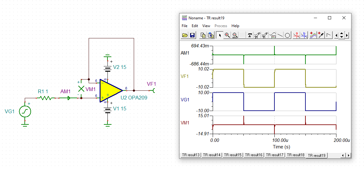
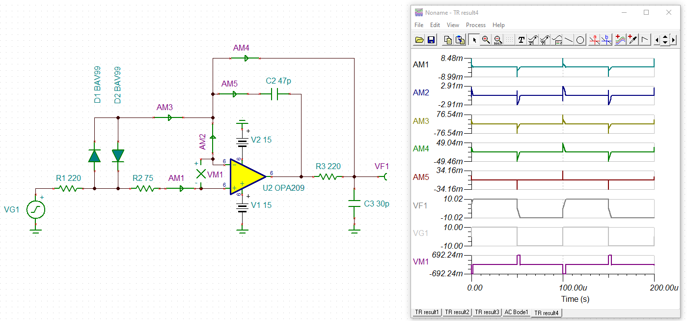
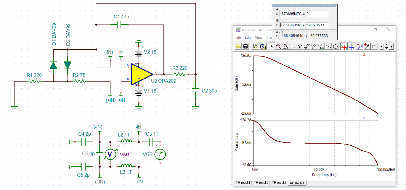
if an op-amp voltage follower is behind a multiplexer, the input voltage of the op-amp might rise or fall faster than the slew rate of the op-amp and current might flow through the input protection diodes towards the output/load.

This current must be limited to a maximum of 10mA.

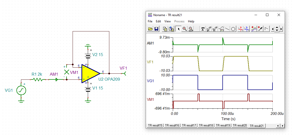
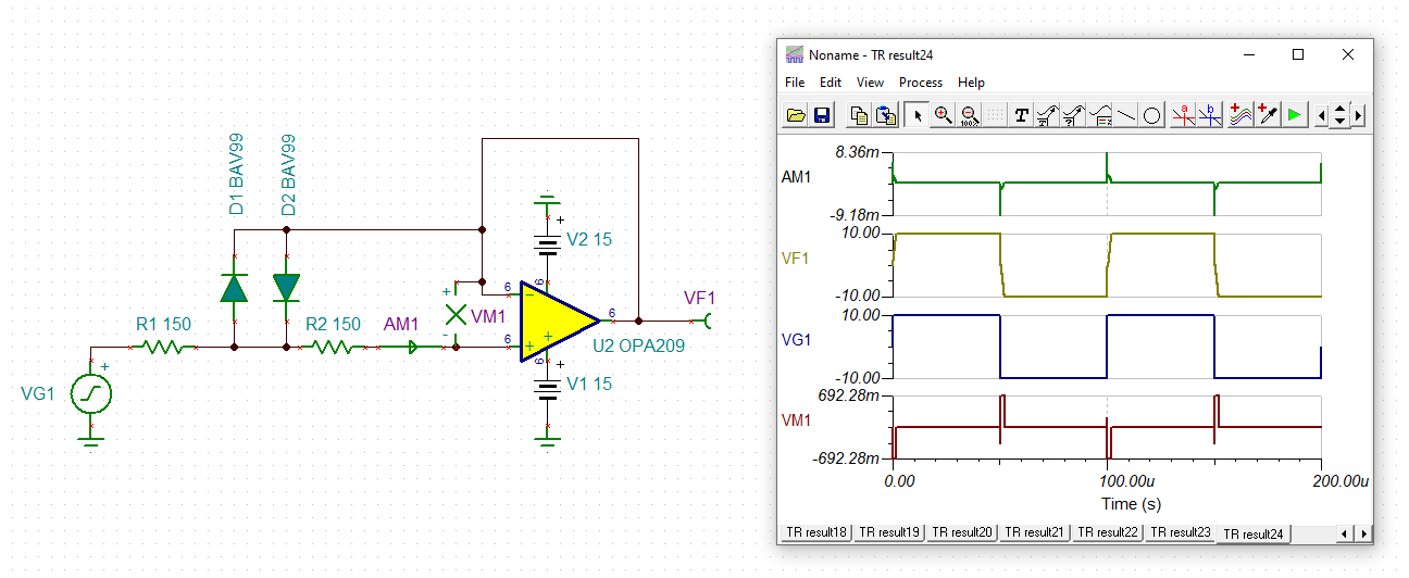
IIRC one can either connect a resistor between the mux and the non-inverting input of the op-amp or a resistor between the op-amp's output and the inverting input (so the series connection of the input and the feedback resistor determine the maximum current through the input protection diodes).

Unfortunately, both resistors would degrade the noise performance.

Can these resistors be omitted if the load has a high enough impedance?

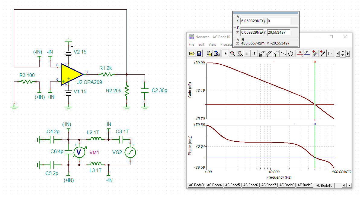
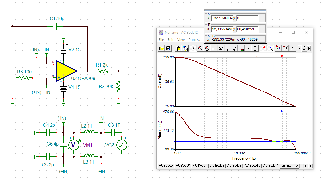
Like if the op-amp would drive a 20k resistive load to GND, even with a +-15V square wave input the current through the load never exceeds 7.5mA, so the op-amp should be safe even without any input- or feedback resistor.

This would mean that the current limiting resistance value would be input-R plus feedback-R plus load-R?

Or would the current through the input protection diodes also flow into the op-amp's output?

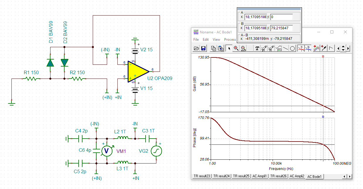
The output impedance of the OPA209 looks like 26µF in series with 3 ohms and 2.4µH, which would result in a 0.78mAs pulse (78ms at 10mA or 7.8ms at 100mA and so on).

Would the input protection diodes (or the op-amp) survive the according energy?

  • Hi,

    you could take one of TI's "multiplexer friendly" OPAmps:

    sbot040b.pdf

    Kai

  • If you give me one with the same noise characteristic in the same package and the same supply and output voltage range...

    Edit:

    And common mode range. I need to "follow" +-15V at +-16.5V supply voltage.

    2k input series R would do with regard to protection, but decreases noise at 10Hz from 3.3nV to 6.6nV/Hz^0.5. Still a bit better than the OPA828 or OPA145, but they also need too much positive supply voltage overhead (and only the OPA145 is available in SOT-23(5)).

    Thanks for the suggestion, though.

  • Hi,

    you could increase the signal amplitude before going into the multiplexer and then use a MUX-friendly OPAmp at the output of multiplexer. By this the signal-to-noise-ratio would remain high.

    Kai

  • I cannot really increase the amplitude of a signal that might be within +-15V.

    Now would the current through the input protection diodes have to charge the op-amp output (in addition to supply the load current)?

    Isn't the output impedance just the relatively high impedance of a current source? At least in RR op-amps?

    How do the 26µF come into place?

    Is this due to some (compensation-) capacitor from the output back to the base electrodes of the output transistors? Or back further into the circuit?

    If this is the same capacitor that limits the slew rate because it must be charged by the input or an intermediate stage, would that help? Or not, because the edge polarities on both sides of this cap are not the same?

  • Hi,

    from these simulations it seems that the current limiting resistor(s) cannot be omitted:

    electron_opa209.TSC

    But an additional diode clamp at the input could eventually do the trick.

    Kai

  • Like this, for instance:

    electron_opa209_1.TSC

    Eventually, R1 should be increased a bit to limit the load current the OPA209 has to absorb.

    Kai

  • Ok, so the current seems to flow into the op-amp and is too high even with a light load or no load at all.

    How about a 2k resistor in series to the op-amp output? If the load is higher than 20k, 15V should still be possible with +-16.5V supply... 

  • Ok, so the current seems to flow into the op-amp and is too high even with a light load or no load at all.

    Yes, the current would fully flow into the output, as the output transistors are turned-on.

    How about a 2k resistor in series to the op-amp output? If the load is higher than 20k, 15V should still be possible with +-16.5V supply...

    The 2k resistor where at the output? In the feedback loop from the -input to the output of OPAmp? This would again increase the noise.

    Kai

  • Just for the record, the OPAmp would be stable with the additional input diode clamp, showing a phase margin of 79°:

    electron_opa209_2.TSC

    Kai

  • Nope, that would be a feedback resistor.

    Just in series with the op-amp output, between the output pin and the load. And the load then connected directly to the inverting input.

    The voltage at the load would be sensed without a noisy resistor and there would be no noisy input resistor.

    The op-amp wouldn't be able to deliver much current, but with +-16.5V supplies it should be possible to drive a load of a bit more than 20k to +-15V.

  • This would also work and reduce the current to a sane level, even without adding any extra noise. But due to R1 and its strong phase shifting effect, you risk to run into stability issues with a capacitive load, way more than when using the diode clamp:

    electron_opa209_4.TSC

    R3 simulates the ON-resistance of multiplexer.

    In any case, when driving an OPAmp with a steep edge, it's good design practise to have a current limiting resistor in the 100R range at the input of OPAmp, to limit the currents running into input capacitance.

    Kai

  • Hello E-W,

    Kai has well covered your OPA209 application questions and concerns. Do you have any additional questions? If not, please go ahead and close out this e2e inquiry.

    Regards, Thomas

    Precision Amplifiers Applications Engineering

  • Could I try to compensate for the phase lag by adding a capacitor in parallel with R1? Of course this capacitor would have to be charged by the current through the input protection diodes, but so would the load capacitor. And it would still be orders of magnitudes smaller than the effective 26µF when looked into the output pin directly. Fortunately, the load capacitor is much smaller than the 30pF you assumed.

    With regard to the 10mA limit for the current through the input protection diodes, this is meant as DC current, right?
    So would a short higher peak be OK (like the current needed to charge the 30pF load capacitance in your model)? And is there any information on what would be safe?

  • Hi,

    yes, phase lead compensation is an option. Keep in mind, though, that even without any load capacitance "C2" the output still sees the input capacitance of OPAmp "behind" R1. So even without any load capacitance a nonvanishing phase lead compensation capacitance will be necessary:

    And any add of load capacitance would have to be compensated with an extra portion of phase lead capacitance. And the higher this phase lead capacitance, the higher the unwanted input current spike. What load capacitance are we talking about?

    You could put a current limiting resistor in series to the phase lead capacitance to furtherly limit the current.

    Have you thought about putting a RC low pass filter at the +input of OPA209 to make the input ramp less steep? 220R and 10n could do the trick.

    Kai

  • I would probably do it with this compromise:

    electron_opa209_5.TSC

    electron_opa209_6.TSC

    Kai