This thread has been locked.

If you have a related question, please click the "Ask a related question" button in the top right corner. The newly created question will be automatically linked to this question.

INA190EVM: Noise performance

Part Number: INA190EVM
Other Parts Discussed in Thread: INA190, OPA320, LM7705

Dear TI colleague

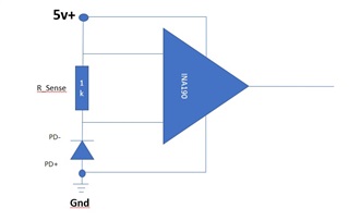
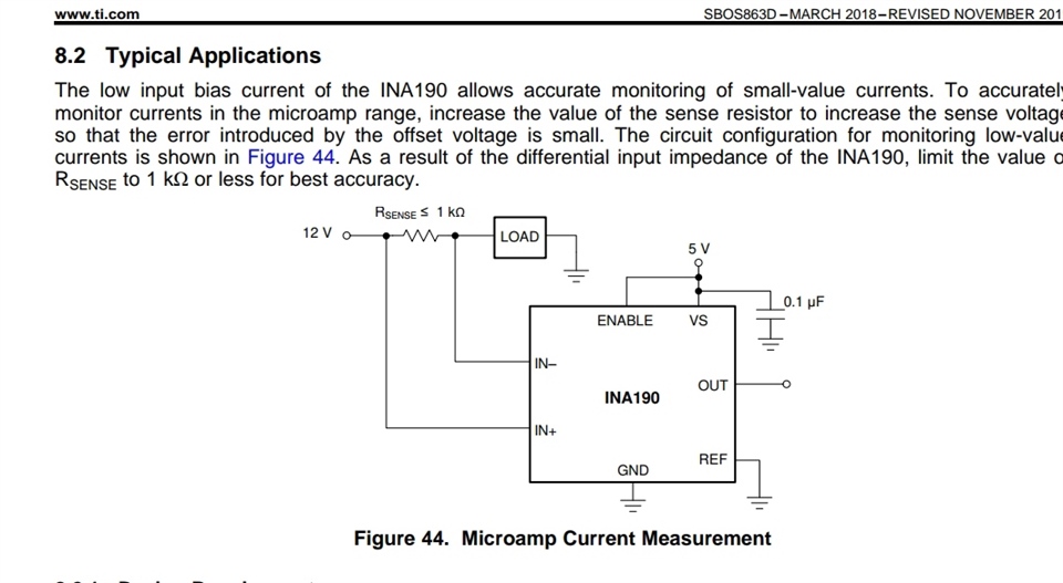
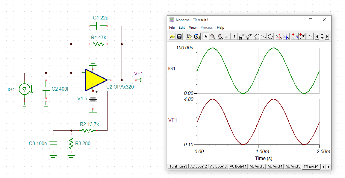
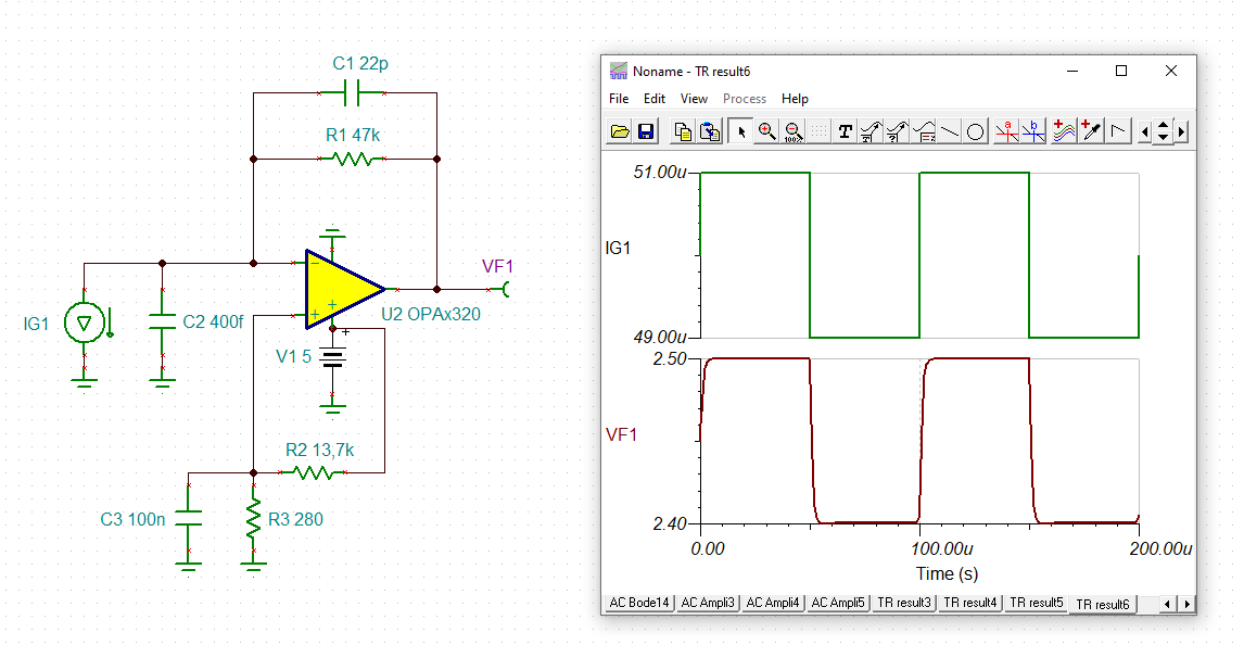
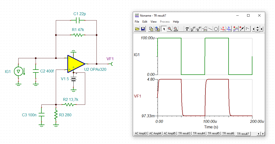
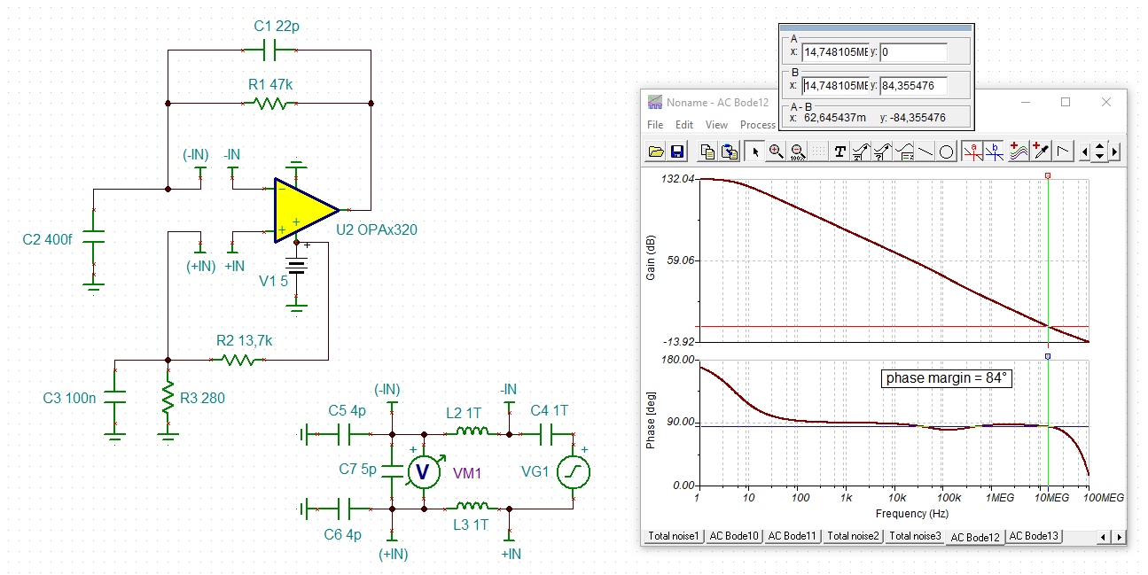
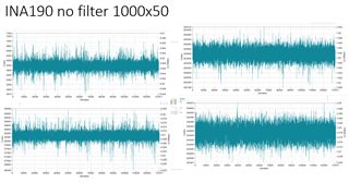
I am using INA190EVM as an amplifier for a PIN photo-detector. The light input is CW light, no modulation is on. The current is below 0.1mA. Rsense is 1k Ohm.  INA190A1 chip is selected.

There is always around 30mv noise exist. May you advise why there is such a big noise there and how to reduce it? thanks very much.

Best Regards

Zhaowen

  • Hi Zhaowen,

    it's very very very unusual to use a current sense amplifier to amplify the signal of a photo-detector. The INA190 is designed to be used in combination with shunts in the milli-Ohm range. In any case we would need a schematic to be able to tell anything useful.

    Why not taking a TIA (transimpedance amplifier) for your photo-detector application? Please tell more about your application and give some numbers Relaxed

    Kai

  • Hi Kai

    Thanks for your comments. We are trying to make an ultra low noise, low bias current, and low offset amplifier for PIN photodetector. We expect the output voltage should be from 0 to 3.3v for optical input  from 0mw to 0.1mw (or current is about 0 to 0.1mA) with output noise level below1mv. 

    The INA190 works well for PD, but the noise is large. The schematic used is as below. 

    Please kindly advice the reason of the large output noise (30mv). You may also advice other suitable IC if INA190 is not suitable.

    Thanks very much

    Zhaowen

  • Hi Zhaowen,

    as I said before you run the INA190 with a way too high shunt resistance for which the INA190 wasn't designed for.

    Here is a much better approach with a TIA. See this very nice appnote:

    tidu535.pdf

    Can you tell more about your application? What photo-detector do you intend to use? What is your frequency range of interest? DC?

    Kai

  • Hi Kai

    The smallest shunt resistance I tried was 50 ohm, but noise is similar.

    Its application is for optical sensing signal detection. PIN diode is used. The frequency range is supposed to be from DC to 100khz. 

    Zhaowen

  • What PIN diode is used? The junction capacitance (detector capacitance) is important for calculating the obligatory phase lead capacitance. Without proper phase lead capacitance the TIA might become instable.

    Kai

  • It's a general InGaAs PIN from a small vendor.

    The capacitance is 0.4pf.

    Dark current 0.3nA.

    BTW, in INA190 datasheet, the shunt resistance requirement is below 1k Ohm. Then why the noise is still high? I am quite confused.

  • Hey Zhaowen,

    I sincerely apologize for my delay. I am looking this over now and will provide response shortly.

    Best,

    Peter

  • Hey Zhaowen,

    • What is the absolute smallest current you are trying to measure and with what PWM frequency and/or duty cycle if applicable. This is fundamental limitation for any current sensing circuit.
    • What is the BW required for this circuit?
    • Do you need to accurately capture a 100kHz signal?

    The INA190A1 typical BW is 45kHz. So this is not a good amplifier to use for a 100 kHz signal. Although device can perform well with DC. Please see this circuit design on how to calculate total worst-case DC error over temperature for INA190A1 measuring 1uA to 104uA.

    The main reason we recommend using shunts < 1kΩ is because we do not want the high shunt resistance to load down the front end of amplifier and the internal switching. However, much of these effects could be mitigated/fixed with an input differential capacitor because this can act as a charge bucket for the switching input. Additionally, adding differential low-pass RC filter can help reduce overall output noise from load noise and/or periodic load transients. See the highlight sections from datasheet below.

    If BW of device is acceptable to signal chain, them I highly recommend putting an input filter with maximum allowable BW to attenuate all noise and keep input switching stable simultaneously. Note the difference in noise data. Then add an output filter (also with maximum allowable BW). Consider an active op amp filter circuit at the INA190 OUT pin as this can also help drive ADCs that require low impedance sources with large BW.

    Hope this helps.

    Best,

    Peter

  • Hi Zhaowen,

    I would do it this way:

    zhaowen_opa320.TSC

    zhaowen_opa320_1.TSC

    Kai

  • Hi Kai

    Thanks very much for your kind reply. And nice to see that the frequency response can be 100khz.

    Did you consider the response speed of photodetector in your simulation? As my understanding, the response speed is lower when PIN works in photovoltaic mode(where there is almost no bias voltage for PIN) than that in photoconductive mode (when reverse bias voltage is applied ).

    Zhaowen

  • Thanks very much, Peter.45khz is okay. The 35khz low pass filters were used at both input and output.

    The INA 190 works well, but output noise (30mv) is high than expected. Fom the datasheet, the noise should be much lower. Just like to find a way to reduce noise. 

  • Hi Zhaowen,

    applying a reverse voltage will decrease the detector capacitance and can allow a wider bandwidth of TIA, because when having a lower detector capacitance a lower minimum phase lead feedback capacitance will be necessary which results in a higher bandwidth. But this is usually only an issue in applications where highest bandwidths are demanded (>100MHz). It doesn't play a relevant role in a 100kHz application.

    Applying a reverse voltage does not relevantly decrease the response speed of photo detector when we are talking about a 100kHz application. This might only be relevant in applications where highest bandwidths are demanded (>100MHz)

    Applying a reverse voltage also shows some disadvantages. It will increase the dark current and by this the noise. Also, the linearity will be degraded and the part to part sensitivity variations will increase.

    If you are looking for a precision circuit, choose a reverse voltage of 0V.

    Without knowing the photo detector I cannot tell more.

    Kai

  • Hi Kai

    Really appreciated for your kind suggestions. It really helps.

    One more question is about the offset voltage (100mv at in+). I would like the output from 0-3.3v. Can directly connect in+ to ground? Thanks

    Zhaowen

  • Hi Zhaowen,

    even a rail-to-rail OPAmp cannot go all the way down to 0V at its output. The OPA320 would leave its linear operation range for output voltages coming the negative supply rail closer than 100mV. See the "open-loop voltage gain" specification on page 8 of datasheet of OPA320. That's why an offset voltage of 100mV is generated in this circuit.

    Also, the following circuit might get problems with a signal voltage going fully down to 0V. But if this would be no issue, you could power the negative supply rail of OPA320 by a small negative supply voltage, for instance coming from the LM7705. Or you could adopt the solution shown in figure 44 of datasheet. In these cases connect the +input of OPA320 to 0V.

    Kai 

  • Hey Zhaowen,

    So the pk-pk noise with 35kHz input and output filters is still 30mV? This is too high. I calculate something closer to 3mV pk-pk. To make sure you are measuring the true operational noise for any amplifier make sure you do the following:

    1. Ensure the amplifier output is operating in its linear region (performance will be best when Vout is in linear region, so > ~20mV). This can be accomplished by adding a bias/reference voltage. For CSA INA190, this means applying some small voltage ~100mV to REF pin. This way the device is always in operating region when load current = 0. For op amp OPA320, Kai does this in his circuits with a resistor divider off the single supply voltage.

    Doing this will make any amplifier fast and perform better by ensuring that the output is never saturated and thus avoid recovery delays.

    It is always better to use low-impedance voltage sources for references, but resistor dividers will still work for INA190, but I would recommend at the least a decoupling capacitor at REF pin to help reduce some to the resistor thermal noise.

    2. Ensure you have proper decoupling capacitance as close as possible to the supply pins.

    3. Use an input filter, especially for INA190. Common-mode filters could also be helpful if the diode voltage is noisy.

    4. Ensure good grounding layout; all ground nodes are common and connected with low-impedance traces/cables. This includes the oscilloscope's earth ground as well.

    5. Try measuring the noise floor of the oscilloscope and probe to understand what noise limitation of the hardware is.

    As for using an op amp transimpedance circuit to achieve a high BW, here is one file showing the steps to make one. Note that if you want Vout to drop to 0mV for no load condition, then you will need a negative supply voltage at V- pin as Kai notes. Note that this is possible to do with INA190 as well, but the overall differential supply voltage (Vs - GND) needs be <6V still. The main advantages to using the INA190 here are low IQ, good DC precision, high-input impedance among CSAs, and being able to measure current on bus voltages up to 42V, independent of its single-ended supply voltage. The enable pin is also nice in that it can simplify power sequencing if you end up powering INA190 with a dual supply such as Vs = +2.5V and V_GND = -2.5V with REF= 0V.

    https://www.ti.com/lit/an/sboa220a/sboa220a.pdf

    Here is all of transimpedance portfolio:

    https://www.ti.com/amplifier-circuit/special-function/transimpedance/overview.html?keyMatch=PHOTODIODE%20TRANSIMPEDANCE%20AMPLIFIER

    Hope this helps.

    Best,

    Peter