This thread has been locked.

If you have a related question, please click the "Ask a related question" button in the top right corner. The newly created question will be automatically linked to this question.

OPA810: Layout question for OPA810

Part Number: OPA810

Hello,

Question: 

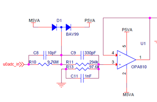
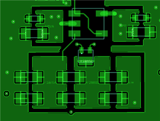
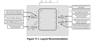
1) Should I remove all the ground under OPA810 from top to bottom layers, including inner GND plane?

2) How to connect front end resistor/capacitor ground? Should it connect through top layer ground ?  Or should I remove top layer ground & go to inner layer GND plan with VIA?

  • Hi Xiaoqiang,

    section 11.2 of datasheet shows a recommended layout.

    Kai

  • Hello Xiaoqiang,

    1. For high speed layouts, it is suggested to remove inner planes around the output and inputs of the device. The opening can just be underneath IN+, IN-, and Out and the component attached to this pin as shown in Figure 11.1 under the section Kai pointed out. 

    1. Preferably, via to ground plane. If this isn't possible, then you may connect it to top layer ground. Top layer ground should have scattered vias throughout board to inner ground. 

    Thank you,

    Sima