This thread has been locked.

If you have a related question, please click the "Ask a related question" button in the top right corner. The newly created question will be automatically linked to this question.

OPA348: offset voltage Vs common mode voltage

Part Number: OPA348
Other Parts Discussed in Thread: TINA-TI

Hello

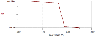
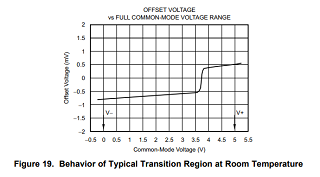
I would like to know how the common mode voltage impact the result.

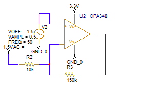
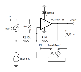
I use a non-invert input circuit. So the common mode voltage could be considered as input voltage. The supply voltage is 3.3V. The signal is a 50Hz voltage signal with 1.5V bias.

Will the offset voltage change with input voltage?

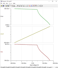
Will the offset voltage multiplied by the gain?

Thanks!

  • Hi,

    section 7.3.2 of datasheet explains what is going on better than I could.

    The "common mode rejection ratio" specification of datasheet says that for best performane the input voltage should stay 1.7V away from the positive supply rail. So your maximum input voltage should be below 3.3V - 1.7V = 1.6V.

    If this is not the case, use a voltage divider to push the common mode input voltage below this limit. Or take another OPAmp, for instance a zero-crossover OPAmp which has an internal charge pump for powering the input stage and is free from these input voltage restrictions.

    Kai

  • Hello Kai

    Please help check whether my understanding is correct.

    If the input signal is less than 1.6V, it will use an offset. And if it is higher than 1.6V. It will use another offset.

    Is that correct?

    Thanks!

  • Hello User,

    Your output voltage will be 1.5V + (VIN + Vos) * Gain  ; where VIN will be your 50Hz

    Note that Vos will change with 1.5V + VIN.  

    If VIN is small then the major Vos change won't happen. So result will be good.

    If VIN is large then the major Vos change will happen. However this change is small compared to the large input. So result will be good.

    It really depends on how accurate the 50Hz signal AC and DC need to be at the output.

  • Hello Ron

    Thanks for your explanation. It is clear for me now. And is it possible to show it by simulation? Did TI pspice model include this impact?

    Could you do a simulation to show me the difference.

    For example, a non-invert input with 16 times gain. Could you show that the output signal may vary from the input signal cross 1.6V

  • User,

    I can help you simulate. Place a voltage meter across op amp input pins. This meter will read input offset voltage. Verify your simulation shows a Vos change.  This is easiest to see with a DC sweep of V2. Then you can export the data and compare output to input * 16.

    Keep in mind that the gain of 16 only supports a signal with 93mV of amplitude. 1.5V / 16

  • Hi,

    If the input signal is less than 1.6V, it will use an offset. And if it is higher than 1.6V. It will use another offset.

    Is that correct?

    Yes.

    In the TINA-TI simulation I don't see any step in the transition region:

    user_opa348_1.TSC

    Kai

  • Kai,

    What is the date in the op amp model [07DEC2011].  Mine is Rev. B   18 March 2003

    Strange that newer is less accurate in this regard

    I did see a shift in mine. Then I expanded the circuit to cover more of user questions 

    Vos versus Bias sweep

    User ,

    With gain 1 , the output error is same as Vos.  Changing R1 to 40k, Ideal gain to 5, and bias to 1.6V

    Sweep VIN -250mV to +250mV.  The output error is Vos * 5 (see below)

    OPA348 Test Circuit.TSC

  • Hello Ron & Kai

    Thanks for your support. It is very clear.

    Thanks a lot!

  • Hi Ron,

    I always take the model from the latest TINA-TI reference design. And, yes, it's [07DEC2011].

    Kai