This thread has been locked.

If you have a related question, please click the "Ask a related question" button in the top right corner. The newly created question will be automatically linked to this question.

OPA192: clarification on operation below max current limit to input pins

Part Number: OPA192

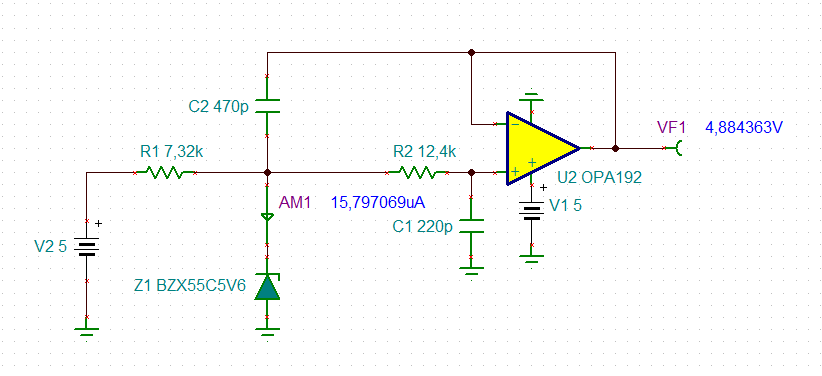
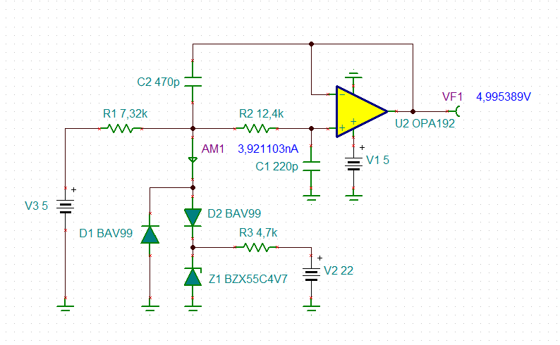
we are currently using a zener diode in our circuit for input pin protection where leakage current in some parts have become a concern. we would like to remove it altogether if possible given the large resistance already in series with the input pins providing current limiting. we have also considered raising the BV of the zener to lower leakage current given global supply chain issues, psecing new parts now is becoming problematic. please let me know asap if the proposed solution is acceptable for our application.

more details in uploaded pdf.

TI ticket.pdf Post

thanks 

Tom

  • Hi Tom,

    Can you describe the characteristics of the input event that you are attempting to protect the OPA192 against? Zener diodes will certainly provide voltage clamping, but can vastly increase the input current of the circuit due to its leakage current and they can add noise and capacitance as well. The are some ultra low leakage current transient voltage suppressor diodes (TVS) that might offer improved performance compared to a Zener diode, but like so many solid state products availability is a major concern or setback.

    Additionally, would you be able to provide a schematic for your OPA192 amplifier circuit? Having the input over-voltage event characteristics and schematic would help us determine if a series input resistor is adequate to protect the OPA192.

    Regards, Thomas

    Precision Amplifiers Applications Engineering

  • Hi Thomas, i dont understand, i already provided the circuit

    please call my cell to discuss

    865-385-5635

  • Hi Tom,

    one way to prevent the high leakage current of zener diode from degrading the performance of circuit is to isolate the zener diode by the help of small signal silicon diodes:

    tom_opa192.TSC

    tom_opa192_1.TSC

    The idea is to bias the zener diode in such a way that the silicon diodes are turned-off almost all of the time. Then only the rather little leakage currents of these small signal silicon diodes have to be considered but not the way higher leakage current of zener diode.

    Instead of the BAV99 even the ultra low leakage current diode BAV199 could be chosen.

    Kai

  • Hi Kai, thanks so much for the clever options. unfortunately our pcb is already laid out and with supply chain issues, if TI can confirm the 600ua current to the input pin is ok w/o the diode, it will alleviate those concerns as well..

  • Hi Tom,

    The former PDF link was taking me to e2e "Create new thread."

    The reposted link to the PDF works correctly. Let me look it over.

    Thanks, Thomas

    Precision Amplifiers Applications Engineering

  • Hi Tom,

    As you have noted in the PDF provided that the OPA192 Absolute Maximum input current rating is ±10 mA. All the OPA192 inputs normally see is the bias current, but if an input over-voltage condition is presented then the input current can rise above normal. That current current flows through one of the input ESD protection diodes which is where the ±10 mA maximum comes about (see datasheet Fig. 65) . If one of those ESD diodes connected from the input to a supply pin does turn on enough to conduct the current, the current is sunk or sourced by the Op amp power supply pin circuit or the supply buss it is connected to.

    A higher than normal input current in the case of your application is 600 uA, which is well below the ±10 mA maximum. And it sounds like that it is only likely to occur as an exception rather than something that happens continuously. The OPA192 Absolute Maximum Ratings do assure that the OPA192 input should be reliable with the 600 uA input current condition. You should be able to remove the Zener protection diode without incurring a reliability concern.

    Regards, Thomas

    Precision Amplifiers Applications Engineering

  • Hi Thomas, thanks so much for the confirmation, this is great news. we will do some additional testing without the diode. can you please confirm also that during this time when the internal protection diodes kick in, there is no phase reversal on the output for this part. from my read of the datasheet, there should not be.

  • Hi Tom,

    All of TI's modern Precision Amplifier Op amps which includes the OPA192 are designed not to phase invert. See OPA192 datasheet Section 8.3.3, "Phase Reversal Protection." 

    Figure 58 depicts the OPA192 non-inverting input being driven +/-0.5 V beyond the supply rails in the example. In this case the ESD protection diodes associated with the non-inverting input are being forward biased and conducting the excessive input current. There is margin built into the anti-phase invert circuit design so you should not see it occur when you do the upcoming testing of your application circuit.

    Regards, Thomas

    Precision Amplifiers Applications Engineering

  • thanks for confirmation Thomas. i appreciate everyone's help