Other Parts Discussed in Thread: INA240
Hello ,
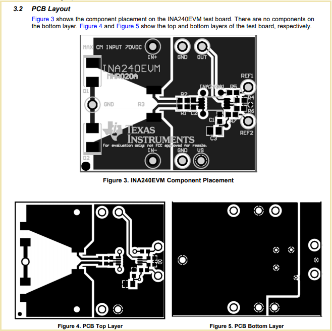
I'm designing a board for current sensing of pwm motor signal. I'm using the Autodesk Fusion 360 to design the board.
When i used the lib for the INA240 to implement the symbol and footprint, i could not connect the INA240 with
the other board signals. The restricted area of the INA was to big. I had two options, using vias directly under the ports
or editing the restricted area by opening the footprint.
So my question is, what is the right way? and if it is making the restricted area smaller, how much smaller do i have to make the restricted area?
Or is it okay for the INA to totally delete the restricted area?
Thank you very much, best regards.


