Hi Team,
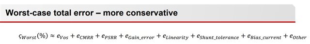
According to the tutorial in TI precision lab, current sensing amplifier's error(worst case) can be listed as below-
% ≈ + + + _ + + ℎ_ + _ + ℎ
However, voltage noise density error isn't listed above, is there any way to calculate the error caused by noise?
Thanks.