This thread has been locked.

If you have a related question, please click the "Ask a related question" button in the top right corner. The newly created question will be automatically linked to this question.

OPA856: DC to 100 MHz Filter design , PSPICE model with PD and design assistance

Part Number: OPA856
Other Parts Discussed in Thread: OPA859, OPA857, OPA855, OPA2837, OPA837, TMUX1109

For test and measurement purposes, a design with switchable gain (x1, x10 and x100) and switchable filter (100 kHz, 1 MHz, 10 MHz, full [>100 MHz])
with high flatness (<= 0.1 dB) from DC to 100 MHz with limited area and power has to be designed.

The design will be supplied with +2.7 V and -2.5 V.
The input and output voltage is at least +-1V peak, higher output voltages up to +- 1.5V or even +-2.0V are welcome.

Currently, the design is in the concept phase.
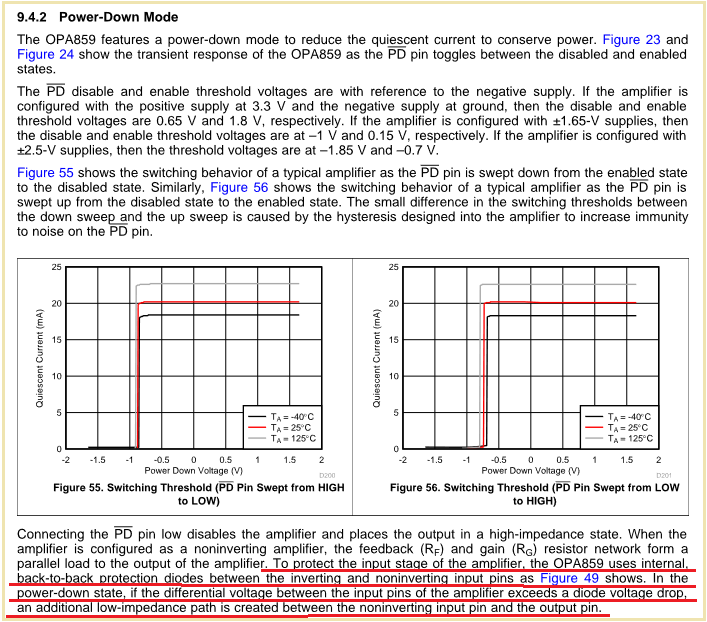
To achieve the goal of eliminating the use of relays, the power-down feature of the OPA85x family will be used. 
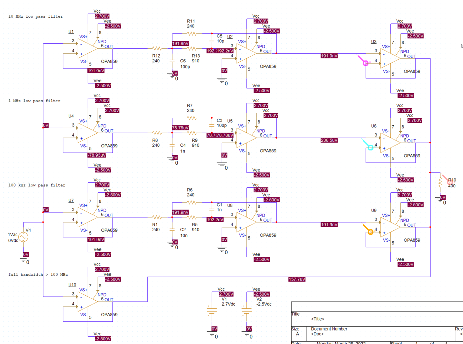
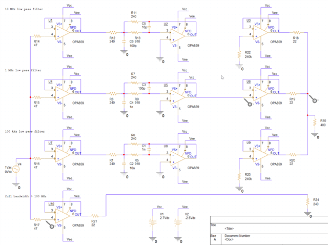
The attached schematic shows 4 parallel filter paths (10 MHz, 1 MHz, 100 kHz, and full bandwidth).
Each filter would finaly contain an OPA856 in its filter path at the input and at the output to disable the path.
When simulating with PSPICE for TI and using the OPA859 model, the following questions came up:

1. is this approach generally usable
    or are there better approaches such as
    a) switchable filter settings or
    b) the use of multiplexers at input and output?
    For an OPA6xx, I remember a recommendation in a datasheet not to use the OPA6xx in a similar configuration for multiplexing.

2. normally I would use the OPA856 as anopamp in the filter stages, but the PSPICE model of the OPA856 does not include a PD pin.
    Is this correct and when will an OPA855, OAP856 and OPA857 model with PD be available?

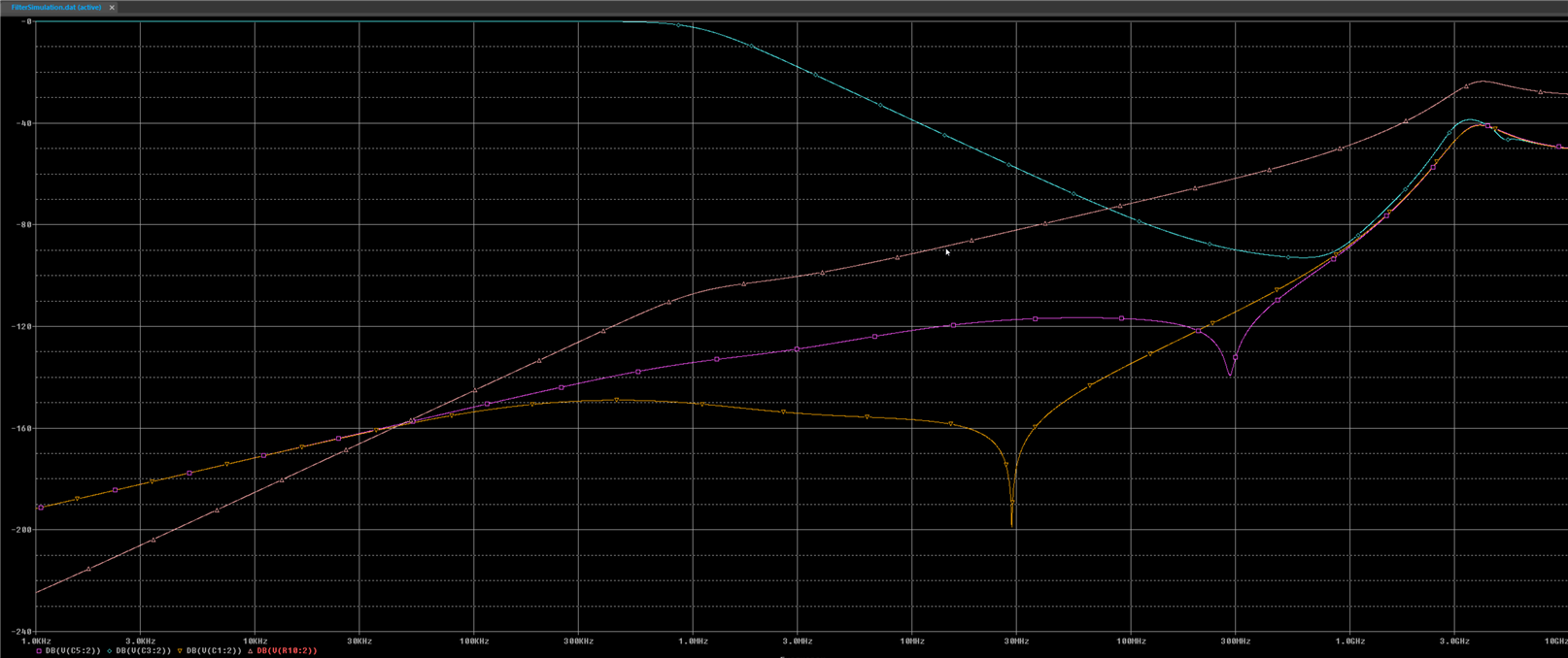
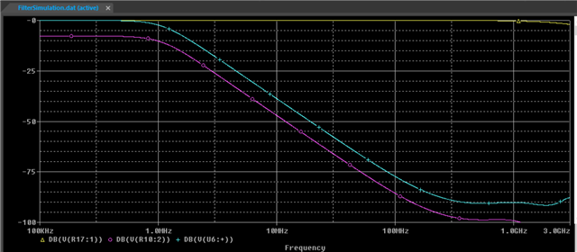
3. in the simulation all outputs of the 4 filter paths are connected to a load resistor (R10, 400 Ohm).
    Even if 3 filter stages are switched off (PD pin at -2.5V) and only the 1 MHz filter is activated
    the output voltage of U6 (equal to the voltage at R10) does not follow the input voltage of U6.
    It looks to me like the output of the deactivated operational amplifiers U3, U9 and U10 is not high impedance
    but force the activated output of U6 down.
    Does this behavior also occur in reality, or is it a limitation in the PSPICE model, and if so, when will it be fixed?

  • Hi Andreas,

    have you noticed that you have mixed up the inputs of all your buffers? Swap the +inputs and -inputs.

    Also, have you already read the red marked sentences in section 9.4.2 of datasheet?

    See also figure 49.

    Assume your input signal is 10MHz. Then the output of your 100kHz low pass filter "U8" will be nearly 0V. In this case "U9" with its input protection diodes will short circuit the outputs of "U3", "U6" and "U10".

    In HF circuits I usually place 10...100R damping resistors directly at the +inputs of each OPAmp. I would do this with "U1", "U3", "U4", "U6", "U7", "U9" and "U10" (after correcting the wiring mistake, of course). This damping resistor dampens the resonance formed by parasitic compex impedances (stray capacitance, internal bond wire inductance, etc). It can often be seen, that only the input stage of an HF OPAmp is wildly oscillating, without affecting the rest of OPAmp. An input damping resistor can reliably prevent such an input stage instability.

    And there should be an 10...47R isolation resistor directly at each OPAmp output. If the OPAmps are sitting close together with their outputs directly connected to the associated inputs, I would do this at least with "U3"," U6", "U9" and "U10", directly at the OPAmp outputs, already in front of R10.

    An example, assume "U2" and "U3" are not connected directly to each other but there is a distance of a few centimeters between the output of "U2" and the input of "U3", then I would place a small isolation resistor directly at the output of "U2" and a damping resistor directly at the input of "U3". Allthough looking like ridiculous over kill, this measure can be extremely helpful to keep a HF circuit stable, especially in big and complex HF circuit with lots of HF OPAmps.

    If the connections between the outputs and inputs become longer and longer, copper tracks begin to form a characteristic impedance which may need to be properly terminated. Microstrip line technique can help then.

    Another measure can often help to enhance the stability: Many OPAmps become unstable when set to a gain of +1 (even unity gain stable OPAmps) and become stable when set to gain of +2. To provide a total gain of +1 a 2:1 voltage divider would have to be installed at the input of OPAmp then. This measure can be helpful in big and compex circuits with lots of HF OPAmps, especially if critical loads are hanging on the outputs. 

    Kai

  • Hi Kai,

    many thanks for the feedback. I had quite often some PSPICE for TI Licence problems so my feedback with a little more than expected delay:

    The intention in this concept phase is to verify if the PD mode of the OPA85x can be used for switching between the diffferent low-pass filters in generell. Your attached underlined explainations (To protect the input stage of the amplifier, the OPA859 uses internal back-to-back protection diodes between the inverting and noninverting input pins. In the power-down state, if the differential voltage between the input pins of the amplifier exceeds a diode drop, an additional low-impedance path is created between the noninverting input pin and the output pin) explains the simulated behaviour. 

    Your feedback with regard to the additional input and output resistors is highly appreciated. Would be the next step once the power down or muxing topic is clarified.


    After resolving the mixedup inputs of all buffers (swap the +inputs and -inputs) and already adding the proposed input and output resistors the simulation has been executed only with one complet low pass filter path (U4, U5 and U6) and just two disabled output stages in power down mode (U3 and U6). Nevertheless U3 and U6 have an inpact to the output signal even if they are in power down mode.

    After some research I found the following document:

       Using Operational Amplifiers as Multiplexers in Cost-Optimized Designs
       https://www.ti.com/lit/an/sboa311a/sboa311a.pdf?ts=1649500359736&ref_url=https%253A%252F%252Fwww.startpage.com%252F
         The second design issue that must be considered is if an amplifier has input clamping diodes. Input clamping diodes can turn on and short the output
         voltage of the enabled amplifier to the input voltage of a disabled amplifier. Figure 5 displays how the input clamping diodes can turn on and conduct. If the
         input clamping diodes turn on two conditions can occur: the enabled amplifier output overdrives the input signal of a disabled amplifier or the input signal of
         a disabled amplifier is the output signal. Therefore an amplifier without input clamping diodes is required. See the MUX-friendly Precision Operational
         Amplifiers Tech Note for more information on the challenges and solutions to input clamping diodes.
       Example: 
          OPA837 / OPA2837
          https://www.ti.com/lit/ds/symlink/opa2837.pdf?ts=1652075659675&ref_url=https%253A%252F%252Fwww.ti.com%252Fproduct%252FOPA2837


    So this means to me that using the OPA85X OPAmps is not possible in the concidered configuration for switching between the different low pass filter pathes
    and relais or multiplexer (like TMUX1109) have to be used. Correct?

    Best regards,

    Andreas

  • Hello Andreas,

      Overall, your explanations are correct, and the OPA85x family do contain input clamping diodes between its inputs.

      I will compile some resources plus additional information, and get back to you soon.

    Thank you,

    Sima

  • Hi Andreas,

    So this means to me that using the OPA85X OPAmps is not possible in the concidered configuration for switching between the different low pass filter pathes
    and relais or multiplexer (like TMUX1109) have to be used. Correct?

    Yes.

    I would take a low capacitance MUX like the TMUX15x.

    Kai