This thread has been locked.

If you have a related question, please click the "Ask a related question" button in the top right corner. The newly created question will be automatically linked to this question.

BUF634A: Can I rebuild jim williams' design (AN18F) of high current booster using OPA207 + BUF634A?

Part Number: BUF634A
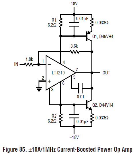
Other Parts Discussed in Thread: OPA207, DAC11001B, DAC91001, TINA-TI, OPA549, LM3886, OPA564, OPA1656, OPA1622, BUF634

Hi, I want to reimplement Jim Williams classic power booster design using all TI's parts. The design is detailed in AN18F.pdf, Figure 2,

Jim Williams AN18F

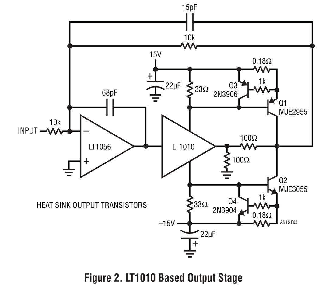
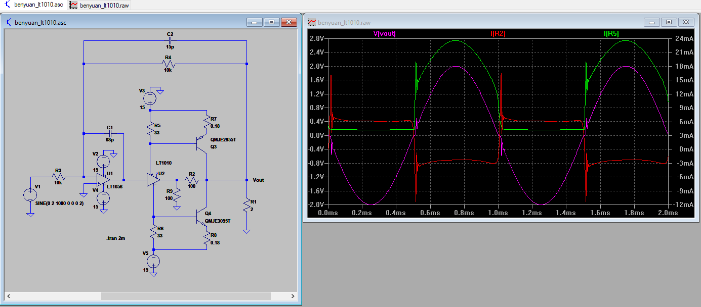
Where LT1010 is working, a current of 150ma Flows over 33Ohm resistors to turn on the Q1 and Q2, which conduct a 3A current to the load. Our application is a large disk coil which requires extreme low THD and fast bandwidth (400KHz, +-15V, >10V/us slew rate, THD<0.0001%).

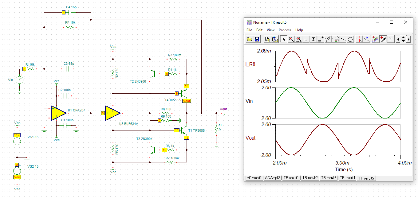
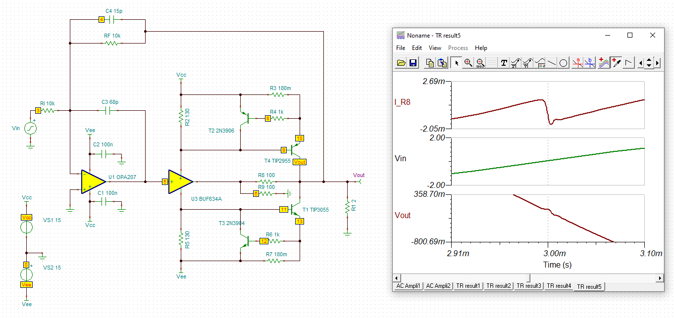
I replaced LT1056 with OPA207 (for better DC performance and a higher bandwidth of 400KHz  with a 10V/us slew rate) and LT1010 with BUF634A. I build the circuit using TINA, OPA207 and BUF634A are from the TINA example designs, MJE2955T and MJE3055T are using the PSpice model from On semiconductor websites. These BJT models are compiled using TINA and import as a micro. The schematic is as follows:

TINA AN18F

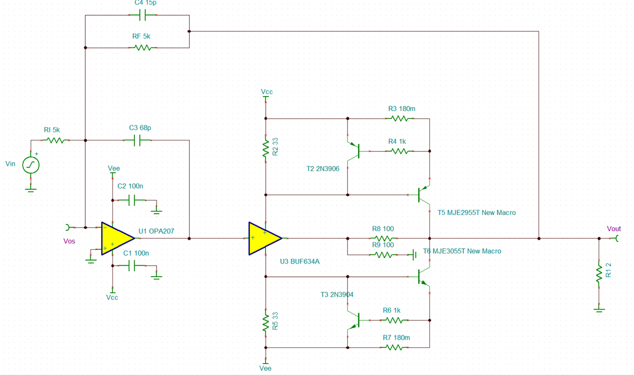
The problem is that the output is 0.

My question is,

1, Can I rebuild jim williams' design using TI's parts? 

2, Will this circuit achieve low THD distortions < 0.0001% and high bandwidth (400KHz)? If so, how could I modify this TINA circuit and how could I analysis the THD metric? Is this power booster free of crossover distortions?

3, If 1 is resolved, I am going to build a PCB to test this design. Is there any guidelines in powering this circuit, as well as protecting the circuit from back EMF?

Thank you.

Benyuan

AN18.TSC

  • Hi Benyuan,

    what is the load current you need? What is the output voltage swing you need? What is the input signal of amplifier? A static sine wave? What is the inductance of the disk coil? What is the interwinding capacitance of the disk coil? Or, by other words, what is its self resonance frequency? Is a cable used between the amplifier and the disk coil?

    Kai

  • Dear Kai, Thanks for your reply.

    I am design a digital controller for driving a Cambridge galvanometer 6220H - 6240H. The galvanometer specifications are,

    6240H

    Usually, 671XX or DC2000 servo is used to drive 6240H, Its specification are

    Two DAC from TI.com is used (we are evaluation DAC91001 or DAC11001, and maybe DAC11001B), we need to control the moving (location) galvanometer precisely, and preferably achieve TRUE 20 bit resolution. Two dual channel 16 bit ADC from analog (AD7380) are used. The input to this current buffer is +-2V, and its driving capability is +-15V, 3A RMS to 10A RMS. We also need to measure the driving current correctly as a feedback to the PID controller.

  • Hello Benyuan,

    1. Yes, you can rebuild a circuit using these parts. I will need to look into the Tina-TI circuit you provided and work on correcting the output by the end of the week.

    2. Unfortunately, you will not be able to determine THD values precisely with simulation. Amplifier models do not include THD performance, but you might be able to determine a comparison or representation as explained in this thread: https://e2e.ti.com/support/audio-group/audio/f/audio-forum/1080843/opa1632-thd-support-in-the-spice-model. It would probably be easier to evaluate transient/AC response in simulation, then build board for THD measurement.

    3. That is a good design choice to include in your application. Schottky Diodes at output of the amplifier to its rails and transient voltage suppressor (TVS) diode from each supply pin to ground. These two threads talk about this protection scheme in detail:
      1. https://e2e.ti.com/support/amplifiers-group/amplifiers/f/amplifiers-forum/987113/lm7372-failure-of-part-in-circuit-when-unpowered
      2. https://e2e.ti.com/support/amplifiers-group/amplifiers/f/amplifiers-forum/1040979/opa564-question-about-back-emf-protection

       Would you be able to provide a block diagram? 

    Thank you,
    Sima 

  • Block Diagram

    Is this block diagram ok?

    Thanks, The figure 55 in OPA564 is great! I tried OPA549HiREL before but I think its distortion is worse than LM3886 (is it right?). And at this time we think a DC servo + mosfet might be a better solution than LM3886 or OPA549?

  • Hello Benyuan,

      Yes, this helps a lot, thanks! I was wondering if the high current buffer refers to the above design and would need to support the listed, and it looks like that is correct. The transistors (MJE2955) chosen in the push-pull stage should hold up to the requirements. 

      No problem, I am glad it was helpful! You can use either device for Figure 55, the most important are the diodes at the rails and at the output to the rails of the device. However, both devices look to have pretty similar distortion specs over frequency and load. 

       Sorry, I have not had a chance to work on your Tina-TI design/simulation. I will look at that next.

    Thank you,
    Sima 


  • I checked the circuit, and I forget to connect VCC and VEE, Now the simulation looks like this: There is a large crossover distortions. Is it right (AN18F, Jim's circuit is wrong?). How could I mitigate this crossover distortion and optimize THD?

    0434.AN18.TSC 

  • Hello Benyuan,

       Thanks for the update! The composite loop should have helped with distortion. At a quick glance, the problem most likely stems from the push pull output stage especially around crossover distortion from "positive" transistor and "negative" transistor from the period between turning on/off between the transistor pairs. This can be adjusted at the base via common-mode voltages or via diodes to tune when one transistor turns on as the other turns off. 

    Best Regards,

    Sima

  • I am not familiar with these tuning techniques, How could I do to improve this? I want to build a large current buffer with precision Vout, with performance similar to those OPA1622 or OPA1656 chips.

  • Hi Benyuan,

    the circuit uses the current relief method. I don't know the exact word in Englisch. In German we say "Prinzip der Stromentlastung". R2 and R5 are critical, because they have to be dimensioned in such a way that the idle quiescent current of OPAmp shall NOT turn on T5 and T6, even not when heating up all the involved components. The LT1010 draws a supply current of about 5.2mA, times 33R gives about 0.17V. So, there's enough saftey margin to not unwantedly turn on T5 and T6. Only when the load current heavily increases, T5 and T6 turn-on alternatingly, making the amplifier look like a class-B amplifier. Until T5 and T6 turn on the BUF634 has to deliver all the load current!

    The BUF634A draws a quiescent current of only 1.5mA. This means that the BUF634A seems to be running in the "low supply current" mode. To achieve the same voltage drop across R2 and R5 with this very much lowered supply current, R2 and R5 have to be increased to about 120R. Due to stability issues in the simu I had to increase R2 and R5 to 130R.

    This is one cause of the crossover distortion you have observed in the simulation. Another issue is that the transistor models in TINA-TI are older and may not be optimal. In cases where the quality of transistor models matter, I would always import the latest models from the manufacturer. In the simulation below I have changed your T5 and T6 to the TINA-TI models of TIP2955 and TIP3055:

    benyuan_buf634.TSC

    Even with these modifications cross over distortion can be seen. I think this has to do with the fact that the BUF634 does not run in the simulation in "high supply current" mode but in "low supply current" mode. Maybe the model of BUF634 can be modified to allow "high supply current" mode?

    To further decrease the cross over distortion you would need to decrease R8.

    Kai

  • Hi Kai,

    1, About the resistor R2, R5, It is sensing the current flowing into BUF634 or LT1010. Can we set R*I to be approximate 0.17V or we could increase R2, R5 for a large margin R*I > 0.17V or more? How could I get an optimal value for R2, R5 as well as the dummy loading resistor R8, R9?

    2, In using this principle, these current buffer, LT1010 and BUF634A, drives the motor under low load (Iout < 150mA) and turn the extra current driving capability under heavy load (150mA < Iout < 8A). Can we assume that this handing over procedure (this 150mA threshold) is smooth?

    3, And does this principle means that any op-amp draws current from the power line can be used in place of LT1010 or BUF634A? The larger the current, the better?

    4, In your circuit I tried with (TIP2955, TIP3055), (D44H11, D45H11), (MJE2955T, MJE3055T) models, the previous 2 works and the last one fails (BTW, I am do using latest spice model of MJE2955T and MJE3055T downloaded from onsemi's website. But the simulation results are different). So is this related to the spice model? Can I trust the simulations in precisely modeling the power line current into BUF634A? I want to put this circuit into practical application, so it is not until we build this circuit can we say for sure it works?

    Thank you!

  • About the resistor R8, I think that ideally there is no current flowing on this resistor, so the output of BUF634A (VF1) and output (Vout) are the same. In this way, what's the function of R8?

    I monitor the current flowing through R2, R5. In the simulation (using D44H11, D45H11), the current seemed unbalanced:

    AN18 Kai using D44H11, D45H11

    And using your (TIP2955, TIP3055), these current are balanced.

    Kai orig

  • Hi Benyuan,

    the current through R8 can be seen below:

    And with zoom:

    Kai

  • Can I complete remove R8 and make this circuit like this? This is also a power (hand over) boost design by jim williams.

  • Hi Benyuan,

    was curious to see how the LT1010 itself would behave in this circuit:

    Hhm, looks like the "current relief method" does not provide the lowest distortion here, anyway which buffer is used. Me thinks that output transistors are too heavy to be adequately driven by the "current relief method". A way better method was to pre-bias the fat output transistors by an additional buffer stage, or by other words to run the output transistors in class-AB mode. The crossover distortion can only be kept low, when the output transistors are partially turned-on, but not when they are running in true class-B mode, like shown above.

    benyuan_lt1010.zip

    Kai

  • I think the best way is to build it out. I will fabricate a PCB and share the THD results. Thanks.

    Benyuan