This thread has been locked.

If you have a related question, please click the "Ask a related question" button in the top right corner. The newly created question will be automatically linked to this question.

INA849: Gain factor split between INA849 and opamp

Part Number: INA849
Other Parts Discussed in Thread: TINA-TI, REF5025, REF3025

Hi Team,

Can you have a look at the following customer question?

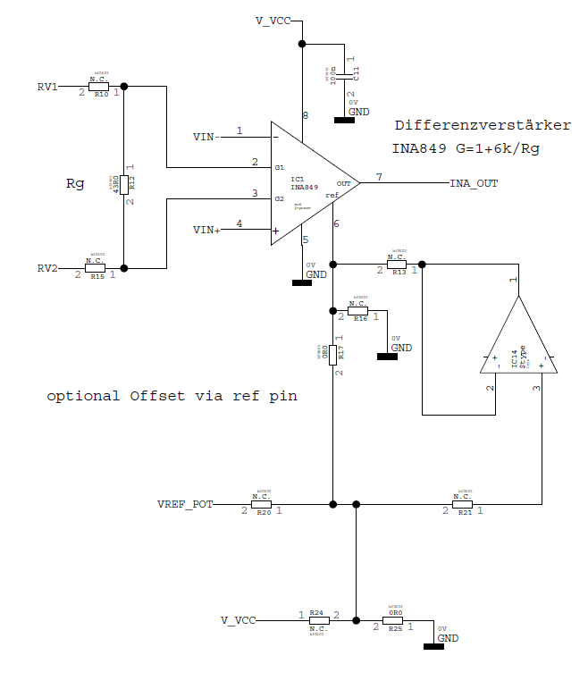
I'm using the INA849 for the evaluation of a strain gauge sensor circuit.
Single supply +15V
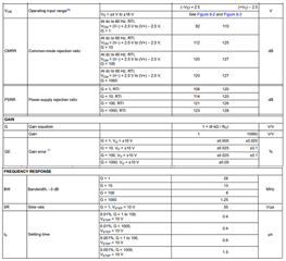
My Vcm is 2.5V. (Sensor is operated with 5 V)
Differential input voltage is between 0.1 mV and ~3.0 mV
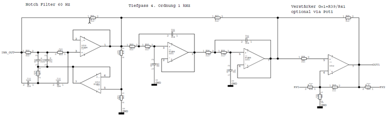
The signal is amplified by downstream operational amplifiers to a range of ~1V - 10V.
(the signal of the INA849 is amplified and ~1V offset is added).

I am still thinking what would be ideal gain on the INA849 and what gain should be selected on the downstream opamp.
And whether the Vcm voltage should be boosted by external circuitry.
At the moment I have the INA849 with G=140, and the opamp with G=20, so that I have a total of G = 2800.

Do you have a suggestion on how best to divide the gain factors?

Thank you,

Franz

  • Hi Franz,

    this depends on the desired overall bandwidth and on what OPAmp is used behind the INA849.

    Strain gauges usually come with very high manufacturing tolerances referring to gain and offset voltage. So, to prevent the amplifiers from clipping, it can be wise not to choose the highest gain.

    Can you show a schematic?

    Kai

  • Hi Franz,

    Do you have a suggestion on how best to divide the gain factors?

    Generally, we recommend to place larger gain in the front stage, if multiple gain stages are implemented. In this case, I would recommend the same. 

    From the IA parameters you provided, the relationship between Vcm vs. Vout is plotted below, which Vcm is not optimized. You may be better off to implement asymmetric dual supply voltage rails in the design. As Kai suggested, could you share the schematic with us?

    You may download the above tool in the link below. 

    https://www.ti.com/tool/ANALOG-ENGINEER-CALC

    Below are the relevant performance vs. gains in INA84 part.  

    If you have additional questions, please let us know. 

    Best,

    Raymond

  • Hi,

    I am the developer of this application with INA849.

    First, It is not possible for me to select the INA849 in the "Analog Engineer Calc" app, as in your screenshot. I downloaded the the version with your link.

    The force sensor is preloaded with a certain force. So I have an offset  value with at least 1.0 mV. The sensor values are all positive and higher than 1.0 mV

    The Ref Pin of INA849 is in current design connected to GND. Rg = 43 Ohm. The output of INA849 is connected to an opamp with Gain of ~25

    The signal of the INA is afterwards optional filtered (notch 60Hz and lowpass 1kHz) and then amplified to max 10V  output.

    The output signal is connected to an input of an analogue  SPS module (0 - 10V). Here at first the sensor is calibrated with 2 points of zero force and maximum force. Software calulates with this 2 reference points the linear equation.

  • Hi Gerald,

    the INA849 is no rail to rail amplifier being able to go all the way down to 0V at the output. The TINA-TI simualtion tells that the output voltage cannot go below 1.5V in your circuit. But with a differential input voltage of 1mV the output voltage should go down to 140mV at a gain of 140.

    So, you would need to add a negative supply voltage to the INA849 or you would need to apply a reference voltage above 1.5V at the REF pin of INA849 and by this create a pseudo ground.

    Kai

  • Hi Gerald, 

    First, It is not possible for me to select the INA849 in the "Analog Engineer Calc" app, as in your screenshot. I downloaded the the version with your link.

    In the analog engineers' calculator, INA84 is listed in the drop down menu as shown below (3rd one). It is not listed in alphabetic order (due to INA84 is more recent IA products). 

    Regarding to your design, I would recommend to increase the INA849's gain up to 1000 V//V in the first stage and balance the remaining required gains in the 2nd stage, say up to 2.8 V/V-> to obtain 2800 V/V. It is possible that you may need to have the large gains.

    As Kai suggested, it will be better if INA849 is configured in dual power supply rails, and/or include Vref voltage at INA84, see the marked key parameters in the captured imaged above. 

    Regarding to 60Hz common mode noise and <1kHz LPF, here are some of suggestions. 

    1. Keep the input transduced leads to be balanced precisely, and keep it shielded from transducer to the input of INA84 (similar to Faraday's cage). If the 60Hz noises are common to both input of INA84, the noises will be rejected from INA849. At Gain = 1000V/V, INA849s CMRR should have >120dB rejection to the common mode noise. 

    2. In implemented differential and common mode input filters, please see the image below in how to calculate these filters. 

    I would recommend to use X2Y filter for the LPF application. In order to increase CMMR rejection, it is recommended to use ±0.1% or better tolerance resistor, including Rg gain resistor value (tolerance down to ±0.01%). 

    https://www.mouser.com/datasheet/2/611/x2y_filter_and_decoupling_capacitors-1771721.pdf

    3.Vref node is a low impedance node, which means that Vref is required to connect to output of precision op amp or REF3025 or REF5025 or similar precision bandgap types of reference voltage sources (capable to source/sink at its output). 

    Enclosed is an INA849's simulation via Tina_TI as an example. If you have additional questions, please let us know. 

    INA849 Force Gauge 04262022.TSC

    Best,

    Raymond