This thread has been locked.

If you have a related question, please click the "Ask a related question" button in the top right corner. The newly created question will be automatically linked to this question.

LMH6554: Silicon Photo Multiplier Summing with differential amp questions

Part Number: LMH6554
Other Parts Discussed in Thread: LMH6703, LMH32401, OPA855, BUF802, LMH6654

Hello,

I am working on a summing circuit for the fast pulses produced by small Silicon Photo Multipliers.  I refer here specifically to the ones from OnSemi (who bought SensL) that feature a Fast output terminal.  Depending on a few different factors the rise time of the pulse is in the 200ps-300ps range.

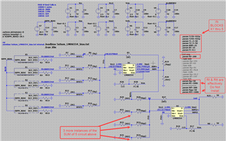
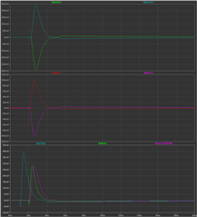
The circuit has 5 inputs to the -ve input of the LMH6554; I fought for a while with some artifacts in the summed signal that I ultimately determined were due to the matching network I had on the +ve input - which, as it turns out wasn't really matching - so I've simply grounded the input and disconnected feedback from the V- output.  And all seems OK, aside from a bit of offset on the output.

So, some questions:

  1. Is there any actual harm to the device from grounding an input?
  2. Are the inputs to this device internally symmetric - that is, could I just as easily sum at the +ve input and ground the -ve?  I ask primarily because of possible advantages during layout.
  3. While I can use the Vcom terminal to to correct my lack of matching, the falling edge of the SiPM actually cross over "zero" - at least with the simulation model I have of the SiPM.  If I want to offset the signal to deal with that cross over, I will have to introduce an offset at the input.
    Would you say it is better to introduce that into summing node or actually add a matching resistor to ground at the +ve input and inject there? In my case I believe that matching resistor will be about 25 Ohms.
  4. Of course I could use a non-differential amplifier but in my previous simulations attempts with other devices I was losing the rise time.  That is, with something like the LMH6703 the rise time is closer to 1ns after the summing (though to be accurate it's actually the fall time due to the summing inversion). Can you think of any other non-differential amp that might do the job?  I've been focused on current feedback amps so I'm not sure if there are other devices with new (to me) technology available now that are just as good for a summing amp.

Thanks
Miles

  • Hello Miles,

    I am going to look into these questions for you; please allow a bit of time so I can coordinate with my team and the analyze the LMH6554.

    Best,

    Alec

  • Hi Miles,

    Can you help illustrate this description with a circuit schematic?

    I think you might need a separate TIA for each silicon photomultiplier, and then have to sum the outputs of theses. Don't they usually need to drive a high-Z input, not just a resistor? The best we can recommend for speed is the OPA855, but it is harder to layout than the integrated LMH32401.

    1. A current feedback amplifier needs to measure the feedback current between the two inputs. I think theoretically you can ground one side and get the right differential output, but the output common mode will have to be off for the math to work out and maintain a virtual short between the inputs.

    2. This amplifier will amplify the current that it measures between the inputs by a large gain. The inputs therefore are an "anode" and "cathode". However, they are symmetrical. You can use either side for single ended to differential conversion, with either inverting and non-inverting gain.

    3. The LMH32401 has an integrated solution, but in this case I believe it would be very easy to reference the other end to a mid-signal voltage to take advantage of the full FDA output swing.

    4. I don't think you should use a current feedback amplifier because it will have a high input bias current. A FET input voltage feedback amplifier will have lower input bias current error for a current measurement.

    I hope I answered some of your questions but loet me know if I missed something. I am curious to learn more about why you have picked this technique instead of the typical OPA855 TIA circuit.    

    Best regards,

    Sean

  • Hi.

    • I do have a schematic, though it is in another SPICE tool (for a variety of reasons not worth going into).  So, I attach some screen shots.  It's probably not the best way to run a Spice tool but my experience with Spice is somewhat limited :)
    • I should reiterate that I realize that I'm not implementing the LMH6654 in a conventional way.  That is, I'm basically approaching it like a conventional op-amp that happens to be very fast and has dual complimentary outputs - which is advantageous.  The result is actually good enough at this point.  Plan to probably use BUF802 to drive out to external equipment.
    • While the SiPM is run "conventionally", we are not looking at the signal from the Anode or Cathode via a TIA.  Maybe we should be, but that's water under the bridge at the moment.  The Fast output is essentially a capacitively coupled output from every (fired?) microcell on the device.  Anyway, I will look at the LMH32401.
    • The second mage is the SiPM circuit block - X5 in this case.  I've got some back termination at the SiPM that I have played with (Bt & BSH).. The values shown in the main schematic are what gives me the best combination of rise time/pulse shape/least wiggle on the back end of the pulse.  It's a compromise... The length of the transmission line is just enough to place the reflection from the SiPM on the back side of the incident pulse.  That is, there is a few millivolt signal at the summing node which seems to be travelling back down this transmission line to the SiPM fast output where it isn't properly terminated.  So, 50 Ohm in series (Bt) would be better, from that point, but the pulse shape is wider as a result.
    • Why this technique... well, we have transmission lines between each SiPM and a common point where we need to sum the signals.  Onsemi has an app note about a Signal Driven Multiplexer technique using fast RF Schottky diodes, and while that works we lose a lot of signal in the process.  There are issues terminating the transmission lines. 
    • Why this technique 2... We've built a multi channel summing circuit before using discrete transistors but it is space and power hungry, and not something we can easily locate inside experimental apparatus.
      There are some custom ASICs that have been created in the physics world to deal with some of these issues but I was hoping to make a (somewhat) quick & (somewhat) dirty circuit to get things rolling... 

  • though I just realized that I haven't gone back and taken a look at a properly balanced circuit configuration - that is with the proper feedback etc to the +ve input  - when I have the back termination at the SiPM.

  • Hello Miles,

    Thank you for providing this information.  We will get back to you with a response next week.

    Best,

    Alec

  • Hi Miles,

    only want to say something general about your summing scheme:

    1. In HF summing amplifiers I always split "Rg" ("Rgg") into two resistors, one smaller one being mounted directly at the output of driving OPAmp and a bigger one being mounted as close as possible to the -input of summing OPAmp. The smaller resistor helps to isolate the output from capacitive loads and to dampen resonances resulting from transmission line effects.

    2. Keep in mind that when summing all too many signals at the -input of a summing OPAmp, the OPAmp's stability can suffer from lots of stray capacitance being built by the many resistors' solder pads and copper tracks being connected together there. Because of that I would remove the ground plane under these signals, especially in the underneath layer. You can easily simulate the effect of this stray capacitance by adding a capacitance from the summing point to signal ground in the simulation. Sometimes it can helpful to reduce the numbers of channels being summed up by a single OPAmp. Of course, this would mean that you have to increase the number of summing stages. But it can help to improve the layout of each individual summing OPAmp and by this the overall performance. Decreasing the number of summed up channels can also help to decrease the noise gain of individual summing OPAmp and by this help to speed up the system.

    Kai

  • Thanks for that. I hadn't thought about #1; I was aware of the points of #2, but layout is not my full time activity so sometimes I forgot the little things that can make a difference, so your comments are a good reminder and much appreciated.

  • Just further comment about this: I did go back and have worked out the proper differential circuit with bias.

    There are advantages to both the grounded +ve input circuit (more gain) and the proper differential circuit, and a lot of that comes down to the proper termination of the transmission lines looking into the summing circuit and looking back out - as those squiggles on the back side of the pulse seems to be related to what the summing node sees (impedance wise) looking back at the multiple sources.

    Since we are primarily interested in the leading edge of the pulse we might be able to live with some squiggles...

  • Hello Miles,

      Were you able to sum these signals into one amplifier with no issues? 

      Proper termination are critical in high frequencies especially with transmission lines. Looks like this is done in the schematic at input and output. Grounding the input is possible, but for fully differential amplifiers (FDAs) we recommend keeping both paths symmetrical or you might run into common-mode issues as Sean mentioned above. This can simply be an equivalent resistor/capacitor at IN+.

    Thank you,

    Sima