This thread has been locked.

If you have a related question, please click the "Ask a related question" button in the top right corner. The newly created question will be automatically linked to this question.

LMP2022: Pin Damage Current During Over-voltage Event

Part Number: LMP2022

Would TI be able to provide the pin damage current for the inverting and non-inverting op-amp terminals?

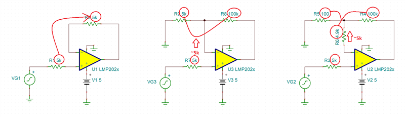
I assume there are steering diodes in the part that protect against over-voltage transients.  I am in an application where I cannot clamp the voltage running to these pins as TVS parasitics affect a sensitive sensor measurement too much.  Therefore, to mitigate overvoltage events, I will place high series resistance going towards the inverting and non-inverting terminals of the pins.  What is an appropriate value for this resistance?

Aidan

  • Aidan,

    You are correct about the existence of ESD protection diodes on each I/O pin of LMP2022 - the diodes can easily handle 10mA dc input current while for transients lasting few microseconds the allowable input current through the steering diodes may be as high as 100mA. Thus, for example, in case of input signal exceeding supply voltage by 10V you should use 1k series input resistor if the signal lasts milliseconds or longer BUT use 100ohm resistor in case of transients lasting just few microseconds.  Since LMP2022 is a zero-drift amplifier with an internal auto-correction circuitry, you should not use a larger input resistor than absolute necessary as this may result in the increase in the input offset voltage and/or offset drift.

  • Thanks for detailed response!

    The transient will last ~300us and peak at 50V.  My circuit can handle added inaccuracy due to input bias current times a ~5kOhm resistor.  This would limit to 10mA during the peal of the transient.

    Aidan

  • Yes, 5k input series resistor will protect the circuit against the damage. If the added inaccuracy caused by R1 is more than you can tolerate, you may improve it by matching two input impedances as shown below.

  • Hi Aidan,

    have you thought about using a diode clamp with a low leakage diode? The BAV199 could be used or the 2N4117/A or the low cost MMBF4117. You would need a current limiting resistor in front of this diode clamp. A resistor between the diode clamp and +input of OPAmp would also be helpful to furtherly limit the current into the LMP2022.

    The advantage of the diode clamp method is that the sum of these two resistances can be made smaller than the current limiting resistance of the single resistance solution.

    Kai

  • Thanks for the suggestion, would the cathode of the diode go to the 3.3V voltage rail that powers the op-amp.  I can see how this would be beneficial.  That said, even moving to a 10kOhm resistor only seems to introduce 450pA*10kOhm = 4.5uV of offset.  This may be close to the consequence of leakage, so I think the resistor is more simple.

  • Aidan,

    Just so you know, the bias current of the LMP2022 behaves differently than a conventional amplifier due to the dynamic transient currents created on the input side of its auto-zero input stage circuit. The input bias current is affected by the charge and discharge current glitches of the input auto-zero circuitry. This effectively creates a repetitive impulse current noise of 100's of pA. For this reason, the LMP202x is not recommended for applications with high source impedances. The amount of current sunk or sourced from the input stage is dependent on the combination of input impedance (resistance and capacitance), as well as the balance and matching of these impedances across the two inputs. These positive and negative input current pulses, integrated by the input capacitance, cause a shift in the apparent "bias current" - because of this, there is an effective "bias current vs. input impedance" interaction. Since the input bias current is dependent on the input impedance, it is difficult to estimate what the actual input bias current is without knowing the end circuit and associated capacitive strays.  For this reason, you may NOT assume that 10kohm input resistor together with 450pA IB would introduce 4.5uV change in the input offset voltage because IB is a function of input resistor and stray PCB board capacitance while datasheet IB spec limit applies only to circuits without any input resistor. Thus, the main reason for matching input impedances between the input terminals is to minimize the input offset voltage shift caused by integrated IB's mismatch.

  • Thank you for the explanation here Marek, I've added balancing resistance in the feedback path of my buffers to compensate!

  • Great.  Please let us know if you need further assistance.