This thread has been locked.

If you have a related question, please click the "Ask a related question" button in the top right corner. The newly created question will be automatically linked to this question.

THS4151: Analog Front End (AFE) Attenuator Circuit

Part Number: THS4151
Other Parts Discussed in Thread: OPA810, THS4551

Hello all, 

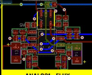
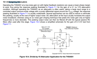
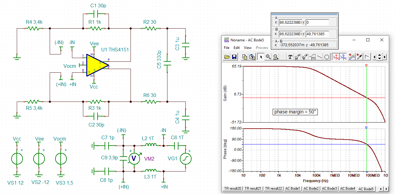
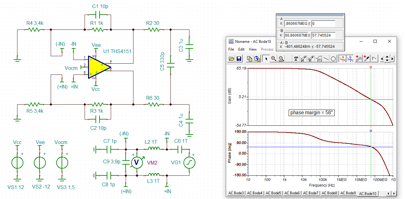
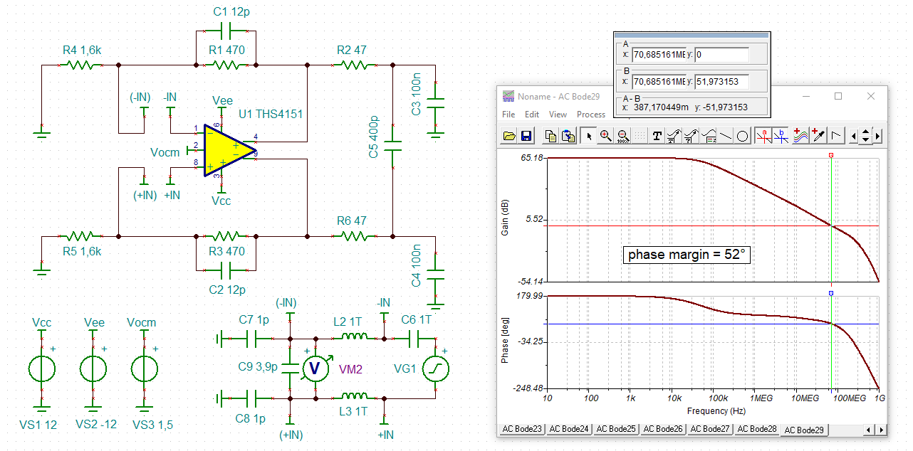
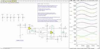
I have simulated the shown attenuator circuit on TINA. The purpose of the circuit is to drive an ADC. The input signal would be a sensor signal ranging from -10V to 10V and the required output that would be input to the ADC would have to range from -3V to 3V. 

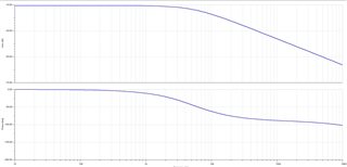
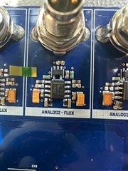
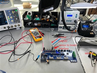
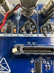
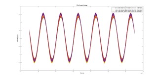
In the TINA model everything is working as I expected, when the circuit however was produced on a PCB, the measurements I would get at the output of the FDA THS4151 were erroneous. 

No matter what the input voltage/(input sensor signal) is, I always measure a differential voltage of 20V at the output of the THS4151. What makes things even more peculiar is the fact that even where there is no input voltage(/input sensor signal), I still measure 20V at the output of the FDA. 

I would really appreciate any inputs and recoomendations that could help me solve the issue. 

Looking forward to a reply. 

Kind regards

  • Hi Kosta,

    I would run a phase stability analysis. C6 and C7 appear to be extremely huge. And C3 and C4 could be too big. Another option is to use the dual feedback method.

    Kai

  • Hi Kosta,

    Can you show me what the input and output looks like on the scope? I would agree that maybe a MFB filter is preferable to those large output capacitors, but since you already have a PCB made we can try to debug. Any snapshots of your test setup, board layouts, etc will help.

    Best,

    Sam

  • Hello Kai, 

    The results I get when I simulate the AC Transfer Characteristic of the differential ouput voltage of THS4151 (assuming this is the analysis you imply when you say "Phase stability analysis") do not seem to show anything problematic. The cut off frequency is around the calculated value which, as far as I can understand, is also influenced by C3 & C4. 

    Just to be sure however I did remove the following caps: C3 & C4 and C6 & C7, and the results I get are the same as previously. So I am not sure about the influence of these capacitors on the performance of the circuit, eventhough I would agree that they are on the higher side. 

    Please let me know if you have any other suggestions. 

    Kosta 

  • Hello Sam, 

    So far I have been testing with a laser sensor which depending on the distance it has wrt to a flat surface gives a certain voltage output. The sensor will be prone to oscillations in the actual application however, for now I have it on my desk at a certain distance wrt a surface. At this distance that I am testing, the output of the sensor should be 5V. 

    Unfortunately, currently I am not at the lab where I usually work, however I can tell you that the input t0 the circuit (that is VG2 and V_unfilt) referring to the TINA schematic is indeed 5V as I would expect. And nothing unusual is noticed in this 5V characteristic. 

    The differential output(Vout_diff referring to the TINA scematic), as I have mentioned before, is 20V and apart form the fact that is the wrong voltage output I would expect, it doesnt show any unusual behavior or transient. 

    Moreover, the output of OPA810 also seems to be correct, so the performance seems to be degrating at the second part of the circuit which is the FDA THS4151. 

    Finally I am sending you some pictures of the PCB layout and test setup 

    Please note that some wrong traces/connections were noticed on the board and these have been resolved. Spcificaly I am talking about the connections between the output pins of the THS and the output resistors. If you refer to the PCB layout, these connections should be between:                               

    NetC69_A5_1 & NetC65_A5_1  

    NetC65_A5_1 & NetC69_A5_1

    These have been corrected by using some jumper wires on the board I am testing with. 

    Moreover, pin 7 is also supposed to be  "NC" in the specific package of THS4151 I am using, and this has also been corrected on the board I am testing with. 

    Finally about the board, this is a prototype board which was designed in order to test and validate the performance of all subcircuits on it, so in that sense I am somehow flexible in redesigning parts of the board however, I would also prefer to just get in the bottom of this issue and actually understand what is causing this behavior. So, some help with trouble shooting would indeed be appreciated. 

    If you absolutely need to see the input and output as shown on the scope, this will have to wait till Monday (May 30th 2022) 

    Looking forward to your reply with any other suggestions and recommendations. 

    PS: If you referr to the answer I have given to Kai you can also see that even after removing the high value caps, the results I got were still the same.

  • Hi Kosta,

    It looks like you have your feedback paths crossed. Could you share the CAD schematic? Did you run a DRC for this board?

    Also did you make sure to cut the traces that you reworked with wires and do a continuity check on the old/wrong connections?

    Best,
    Sam

  • Hello Sam, 

    The feedback paths are crossed indeed. The connections were wrong on the scehmatic as well and so, the DRC did not report any violations for this detail. The traces I reworked with the wires were not actually cut, but what I am doing is placing the resistors vertically on pads ANALOG5_P and ANALOG5_N (referring to the PCB layout picture) and the other side of the resistors I solder directly on pins 4 and 5 of the THS4151. Therefore, I bypass the pads that have been wrongly traced to pins 4 and 5 of the THS4151. 

    I hope this gives an answer to your question. 

    I really think that all the connections should now be correct as I am also continuously checking them to see if anything is disconnected or not connected correctly.

    Things however still seem to not work which really puzzles me. 

    I hope to hear from you soon. 

    Best regards,

    Kosta

  • Hello Kosta, 

    Well if your feedback traces were crossed physically, there is some chance you damaged the part. in any case, one of the wonderful things about FDA's is you can design attenuators using much lower supply devices as they will level shift everything to your desired output Vcm and Vpp. I put a section on "Designing Attenuators into the THS4551 datasheet, in this document, 

    https://www.ti.com/lit/ds/symlink/ths4551.pdf

  • Hello Michael, 

    Thank you for your feedback. I will take a look at the document you sent me. 

    In the meantime I wanted to ask you the following: 

    You are saying that if the feedback traces were crossed physically, there is  some chance the part is damaged. Would this happen even if the the circuit does not get any input from the sensor. 

    I have to explain that there are 5 identical circuitries in my board and I have tested only with 2 of them. So again, would the wrong tracing result in a damage of the part even if that particular circuit was not used for testing? 

    Looking forward to your reply and any other recommendations. 

    Best regards, 

    Kosta 

  • Just powering them up puts them into a saturated condition with crossed feedbacks, If you have corrected that, try a new part in the corrected layout. 

  • Hi Kosta,

    the phase margin of your circuit is 50°:

    kosta_ths4151.TSC

    50° is a bit low but still acceptable. If you want to improve the noise margin, which I would recommend, then you can decrease the 30pF caps in the feedback loop a bit:

    There's another issue: The two 1µF caps behave like a short circuit at the higher frequencies. At 10kHz the impedance of a 1µF cap is only 16R, at 100kHz only 1.6R, and so on. So you may overload the output at higher frequencies.

    Kai

  • Hello all,

    I would like to let you know that after reviewing the design and working it out on a breadboard, it seems to be working very well.
    It seems that the only major mistake I had made was cross-connecting the feedback paths. It also seems that having the feedback paths cross connected would also result in a saturation of the ICs even when they are simply activated
    without any load. So @Michael Steffes, you were right about that. Thank you.

    I did however notice some noise at the output voltage measured between pins 4 and 5 of the FDA.
    I attempted to decrease the noise by doing the following:

    1. Decreased the Rf and Rg resistors from 1kOhm & 3.3kOhm to 100Ohm and 330Ohm respectively.
    2. Increased the Ccm capacitors from 0.1uF to 0.2uF (in the initial design they were 1uF, but I was told that is too much)
    3. Increased the Diff Cap at the output of the FDA to 400uF from 300uF

    These seem to decrease the noise at the output of the FDA, but I was wondering if there is anything else I could try.
    Perhaps a different feedback method?

    Looking forward to any suggestions.

    Best regards,
    Kosta

  • I am pretty sure now that is what happened. Thank you for the detail

  • Hi Kosta,

    I did however notice some noise at the output voltage measured between pins 4 and 5 of the FDA.

    What noise? HF noise or LF noise? Any numbers or scope plots?

    The 30R / 1µF output low pass filter has a corner frequency of 5.3kHz. This is quite a lot.

    3. Increased the Diff Cap at the output of the FDA to 400uF from 300uF

    300µF ?? Your schematic is showing 330pF.

    Kai

  • Hello Kai, 

    I am sorry, that was a typo. The Diff Cap at the output of the FDA is indeed at pF magnitude. So I tested with 300pF and later on with 400pF. 

    Regarding the 30R/1uF low pass filter: Since I was limited on the type of components I could use on the breadboard,  I have been using a 47R resistance instead of the 30R. As for the 1uF cap, I followed you recommendation and decreased it quite a bit. I have now been testing with 0.1uF and 0.2uF. 

    Here I am attaching the figure that shows the different behavior for the 4 tests I conducted.  

    I was expecting the output of the FDA to swing between 1.5V and -1.5V which it does, however I would also expect that this signal can be somewhat "cleaner".

    I am now assuming that the input (sensor) signal will have a fundamental frequency not higher than 10kHz. 

    Would you suggest to design the filter such that it has an even lowe corner frequency, say around 1-2kHz? 

    Best regards, 

    Kosta 

  • Hi Kosta,

    could already be a stability issue. Because of that I recommended to decrease the feedback capacitances from 30pF to 10pF. Improved noise margin -> less noise. Should be checked !

    Kai

  • Hey Kai, 

    Well that is also something else that I considered based on your last feedback some days ago. The feedpack capacitors are currently 10pF each. This has remained constant in all 4 tests I have conducted. 

    I could increase this capacitance and just see if it would actually contribute in the total noise at the output of the FDA but this would be just to satisfy my curiosity. 

    But in order to decrease the noise at the output of the FDA, would it make sense to go even lower in capcaitance? Maybe 5pF or even less?

    Could be a test that I could easily conduct, provided that I receive the parts first. 

    Curious to hear what you think.

    Thanks again for you interest. 

    Best regards, 

    Kosta 

  • Hi Kosta,

    the feedback capacitors are critical here and must lie within a very narrow range.

    And it is not possible to decrease the feedback resistors all too much, as this would also decrease the phase margin, even with optimally chosen feedback capacitors. Please run my simulation to see what's going on.

    Kai