This thread has been locked.

If you have a related question, please click the "Ask a related question" button in the top right corner. The newly created question will be automatically linked to this question.

THS4012: Problem with working temperature

Part Number: THS4012
Other Parts Discussed in Thread: THS4032, OPA2690, OPA2691, THS4011, TINA-TI, OPA690

Hi Team,

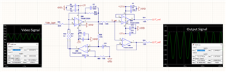
I have created an 4 channel double isolation for analog video signal (CVBS). After optoisolation I have a video signal 1Vp-p with 9V offset
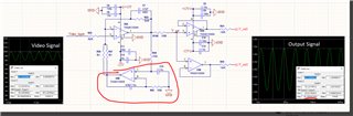
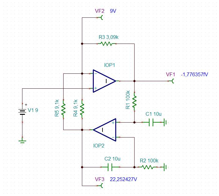
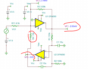
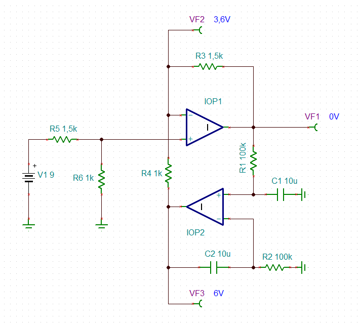
To remove this offset I have used o pre-amp base on 2 x THS4012 on each channel. 

The problem is a high temperature of the component in 25 deg. C it's 65 - 70 deg. C. 
Maksimum working temperature of this device is 50 deg. C so I'm worried about service life because THS4012 in this ambient temperature has nearly 100 deg. C.
On PCB I have total of 12 ampliefiers so inside the chassi is realy warm. 
I have a big 4 layers PCB: Top (signals without plane), GND, VCC, Bottom (with GND plane) and ampliefier has powerpad connected to GND by 4 via. 

Do you have some idea how to reduce temperature of this component? 
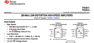
THS4012 is a high speed amplifier with 290 MHz bandwith and I wonder if using worse amplifier with smaller bandwith e.g THS4032 can help?

Thank you in advance.

Best Regards 
Michal

  • Hello Michal,

      Would you be able to share a schematic of the components around the amplifier (mainly input/output/gain configuration) either on this thread or privately via E2E messaging. 

      Is the amplifier working as intended, but the ambient temperature of 100 deg C and a junction temperature was measured at 65-70 degree in room temperature?

      If the above is true, we will have to suggest another device with a higher TA range since the THS4012 is specified at -40 to 85 C. The THS4032 will have the same issue. A schematic would help us suggest a better amplifier for your application.

    Thank you,
    Sima

  • Hello Sima,

    Thank you for your response.

    In my application the maksimum temperature is 50 C. 
    What I measured:
    in room temperature a junction temperature is 65-70 C.
    in ambient temperature 57 C a junction temp is 100 C. 

    I tested that the amplifier could work properly in even higher TA but I'm worried about service life in this application.

    Best Regards
    Michal

  • Hi Michal,

    hhm, 0V at the output of U6A and +9V at the +input of U6A would mean a voltage of +22.25V at the output of U6B?

    Why not doing AC coupling by the help of a suited capacitance?

    Kai

  • Hi Kai,

    I don't understand how you calculate the output voltage on U6B?

    A capacitors isn't a good idea because it created a integrator on video signal. The consequence is the loss of the sychronizing point. 

    If you display on screen a white squar on black backgraound, then you can see some distorsions.

    Michal

  • Probably need to work on your circuit 1st, then your Tj issue will go away, I see you are using LTSpice here, interesting - 

    Anyway, it seems you are using +/-12V supplies only because of the high input common mode, then stripping that off with the integrator around the 1st stage centering up the swing on 0V then simply buffering that out - most of your power is that +/-12V supply which is probably unnecessary for only a 3Vpp swing in the signal. 

    Also, your 3Vpp 30MHz signal is right at the available slew rate for the THS4012, so not a good part to be using anyway. 

    So, you could do this with +/-5V supplies - but, you would need to run both stages as inverting stages to do the level shifting in the 1st stage inside the supply range. A quick guess on parts (as the 1st dual needs to be VFA for that integrator and feedback C to work) perhaps the OPA2690. Your output stages need to be inverting gain of 1 to get back to overall non-inverting. There, most folks would be using a CFA part like the OPA2691. Both of these have plenty of slew rate for your signal and will consume far lower power on +/-5V supplies. Incidentally, your integrator feedback around the 1st loop is a nice way to recenter to ground, but is of course effectively AC coupling the path - just at a very low freqency. 

    Incidentally, the THS4011/4012 datasheet front page still has this ancient error on the front page, that slew rate should be usec, not msec. 

  • Hi Michal,

    I don't understand how you calculate the output voltage on U6B?

    For instance by running a TINA-TI simulation:

    michal_ths4012.TSC

    Kai

  • Well, and taking Kai's file for a start, we can adjust this to a +/-5V OPA2690 solution as thus, we would need to increase the gain for the DC servo path to keep its output in range, that will of course be increasing the NG reducing the BW for the now inverting signal path, but here all the nodes are in range for a +/-5V solution, 

    The SSBW here is this, about 150MHz - 

    With this file, 

    Level shifter with OPA2690.TSC

    And then adding the output drivers - could use the OPA2690 again, but the OPA2691 is a little better slew rate and power efficiency, lots of placed to adjust gain and response shape here and all within +/-5V supplies, down to about 130Mhz now, but pretty flat through 30MHz, 

    and this file, 

    Level shifter with OPA2690 and OPA691 inverting driver.TSC

  • Hi Michael,

    I really appreciate your support

    The circuit which I have created I copied from the internet. I thought that I understand how the circuit work. I have to admit I was wrong.

    I have never used TINA-TI before so it took me some time to properly run a simulation. Anyway, I have some question. From original circuit I don’t understand how resistor R53 and R56||R57 may act  on offset?
    How Is it possible that Kai measured around 22 V at the output of U6B? Last question is to the second design based on OPA690. If OpAmp has supply ±5 V why you can connect signal with 9 V offset to the negative input of the OpAmp?
    Does it cause damage on OpAmp?
    Could you be so kind and explain to me these three things?

    Michal

  • Hi Michal,

    The circuit which I have created I copied from the internet.

    Can you show from where?

    How Is it possible that Kai measured around 22 V at the output of U6B?

    This is a simulation with an ideal OPAmp not needing any supply voltage. Because of that the output voltage of DC servo is 22V. I guess in the original circuit the DC voltage at the +input was way lower than +9V? Then, the output voltage at the DC servo will also be lower and probably well within the output voltage range of U6B.

    So, why not mounting a voltage divider at the input of U6A?

    From original circuit I don’t understand how resistor R53 and R56||R57 may act  on offset?

    The purpose of the DC servo (U6B) is to zero the voltage difference between the +input and -input of U6A.

    Kai