This thread has been locked.

If you have a related question, please click the "Ask a related question" button in the top right corner. The newly created question will be automatically linked to this question.

INA240-Q1: output is abnormal

Part Number: INA240-Q1
Other Parts Discussed in Thread: INA240

Dear team,

We found another phenomena  of the IC as below:
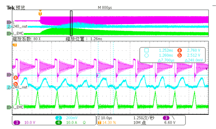
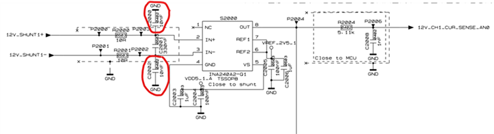
        Test setup:

        Short IN+&IN-, waveform @IN+&IN- is the purple , the ringing is 12V±6Vfrequency 2MHz

        Then test the output of INA240, we found a larger output voltage.

        Question

  • Could you help to explain it
  • Could you help to do a simulation and a test based on this input common voltage.

Thanks & Best Regards,

Sherry

  • Hello Sherry,

    I am looking this over and will respond shortly.

    Best,

    Peter

  • Hey Sherry,

    The INA240 output disturbances can be expected when its input voltage is being switched like this. According the AC CMRR plot in datasheet (Figure 7-12), the device's input CMRR is approximately 65dB at 1MHz VCM switching. With the +/-6V VCM amplitude, I calculate the output offset from VCM to be:

    Vos_RTO = 50 * (12V)*10^(-65dB/20) = 337 mV pk-pk.

    The provided scope shot shows Vos_RTO to be 248 mV, which less than it could be.

    Customer could try to decrease the cutoff frequency of the input common-mode RC filters (R2000&C2000 and R2001&C2002). However, this usually means increasing C2001 (differential) as keeping RC for the differential filter > 10* RC_common mode is best practice. However there are more possible system limitations here such as exceeding bus capacitance or slowing down shunt voltage acquisition. Best practice is to maximize the input filter's fc_differential up until the required system BW. Then choose C2000 and C2002 to be 10x less than Cdiff. 

    Also place a RC filter (with fc less than minimum required system BW/response time) on output as well.

    Hope this helps.

    Best,

    Peter