This thread has been locked.

If you have a related question, please click the "Ask a related question" button in the top right corner. The newly created question will be automatically linked to this question.

OPA2376-Q1: measured offset voltage is larger than calculated.

Part Number: OPA2376-Q1
Other Parts Discussed in Thread: OPA2376,

Dear Specialists,

My customer is evaluated OPA2376 in the customer's circuit, offset voltage is larger than the calculated value.

I would be grateful if you could advise and make a friendship.

--

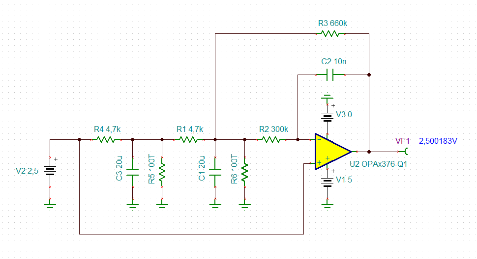
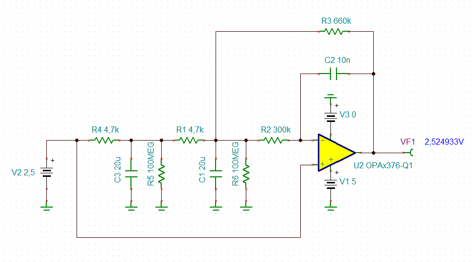
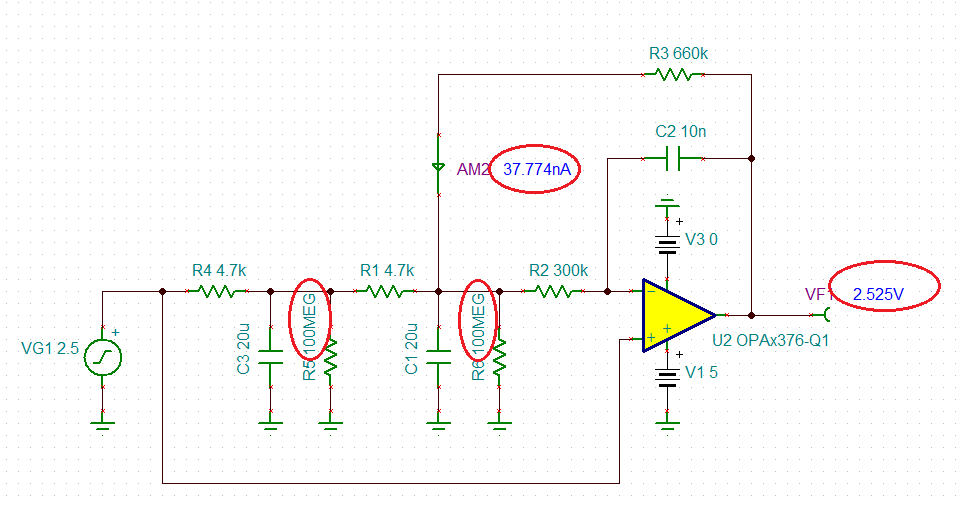
In an inverting amplifier circuit with an amplification factor of about 70 using OPA2376QDGKRQ1,

When the same voltage was applied to the input and non-inverting input terminals as shown in the file below, an offset voltage was generated higher than expected .

application circuit.pptx

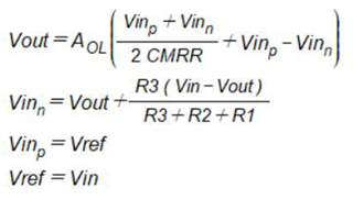
When I calculated the offset current, offset voltage, resistance tolerance, temperature characteristics, PSRR, and CMRR of the inverting / non-inverting input terminals,

the result was that CMRR dominates the offset voltage of Vout.

When the calculated CMRR was the worst, the offset voltage was about 30 mV, while the actual measurement was 60 mV.

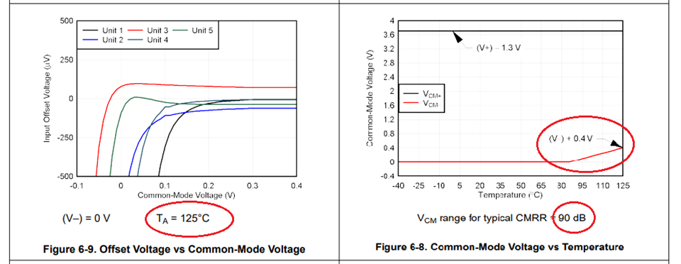
1) Is it possible to drop below CMRR = 90 dB at a common mode voltage of 2.5 V and T = 25 ° C?

2) Do you have the following idea about the relationship between CMRR and output voltage?

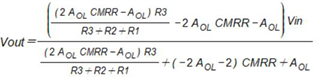
* I ignored R4 and capacitors because I was thinking of applying DC.

Could you please tell me what Figure 6-9 means?
Does it mean that an offset voltage is generated when both the inverting input terminal and the non-inverting input terminal are low and the common mode voltage is close to 0?

---

 For more details of the measurement results, we will send you after making a friendship.

I appreciate your great help in advance.

Best regards,

Shinichi

  • Hi Shinichi,

    hhm, I don't think that this has to do with the common mode rejection of OPA2376:

    But it seems to have to do with the both huge 20µF caps. Such huge caps don't have very high isolation resistances. Or there could be some dirt on the printed circuit board from the soldering decreasing the isolation resistance of caps:

    shinichi_opa2376.TSC

    Kai

  • Shinichi,

    Adding to Kai's comments, OPA2376-Q1 default conditions used in production final test sets Vcm=Vs/2, which would mean Vcm=2.5V on Vs=5V - exactly what you have.  Thus, the maximum offset of +/-25uV applies here and there is no need for accounting of CMRR related error.  Therefore, I think Kai is exactly correct that the error must come from the current leakage of 20uF input caps and/or PCB residue left from soldering - see below example of what happens when accounting for 100M instead of 100T resistors.

    As far as Fig 6-9 goes, it shows five random sample units of the increase of offset voltage at Ta=125C for Vcm within 0.4V of negative rail (V-).  It is closely related to Fig 6-8 showing the increase of offset voltage above 85 deg C.  However, Vcm in your application is at mid-supply (Vcm=2.5V on 5V supply) and thus has nothing to do with this issue.

  • Hi Marek,

    Thank you for your reply.

    I understand the offset is related with the leakage of the 20uF capacitor or PCB leakage.

    I'll share this information with the customer.

    When they have an additional question, I consult you again.

    I appreciate your great help and cooperation.

    Best regards,

    Shinichi

  • No problem.  Always happy to assist you.