This thread has been locked.

If you have a related question, please click the "Ask a related question" button in the top right corner. The newly created question will be automatically linked to this question.

PGA207: Digital grounding connection to analog GND

Part Number: PGA207

Hi team,

For PGA207 layout, here is an design item want to confirm with you.

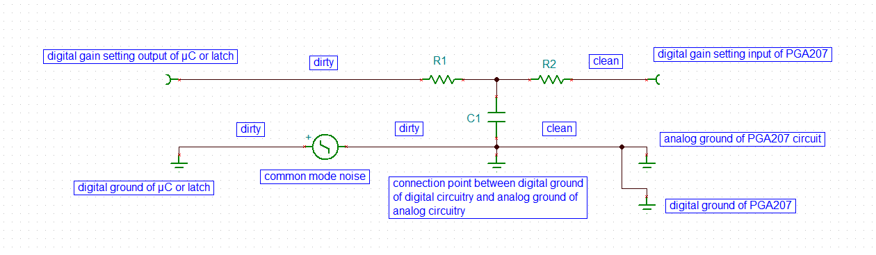
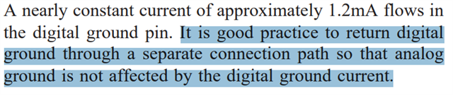
There is a description as following saying the digital ground should return through a seperate connection.

But for the real case, my customer want to know whether they could use one GND plane directly for simple layout? If there is any side effect here?

Thanks

Best regards

Mia Ma

  • The resistance of the ground plane is not exactly zero, so the digital ground current will generate a voltage drop, so the ground pins will not be at the same voltage as the power supply ground. This offset is no problem for digital signals, but might or might not be a problem for the analog ground in the customer's application.

  • Hi Mia,

    The PGA207 has high impedance, differential inputs.  This allows to sense the positive and negative inputs of the sensor or differential signal that is being measured in the application.  The output is referred to the reference (Ref) terminal which is in many cases grounded.  Care must be taken to ensure the I-R voltage drops do not affect the accuracy of the reference pin or the sensitive sensor signals.

    The PCB board layout designer must consider the current return path to GND to ensure any I-R voltage drops across the GND path do not affect the sensitive analog measurements.  In general, we recommend a single ground plane while keeping the placement of the digital and analog portions of the circuit on separate areas on the PCB, keeping the sensitive analog away from noise sources and digital signals.  Although the PCB board layout uses a single GND plane, the key is to keep the current return paths on different sections of the board layout.

    The following application notes may be of interest:

    https://www.ti.com/lit/an/slyt499/slyt499.pdf  

    https://www.ti.com/lit/an/slyt512/slyt512.pdf 

    https://e2e.ti.com/blogs_/archives/b/thesignal/posts/grounding-principles

    Thank you and Regards,

    Luis

  • Hi Mia,

    the 1.2mA DC current is your least problem. Much more important is that you must consequently hinder any digital noise (HF-noise !) from arriving the PGA207. This can be noise on the digital GND pin of PGA207 relative to the analog signal ground of PGA207 circuit or any digital noise arriving the digital gain settting inputs of PGA207.

    So, what to do?

    1. A good idea is to connect the digital GND pin of PGA207 to the analog signal ground close to the PGA207. This forces the digital GND pin of PGA207 to exactly the same potential as analog signal ground and no digital noise can be injected into the internal PGA207 circuitry and by this ruin the signal integritiy.

    2. Unfortutanately, this is only half the job, because digital noise can still reach the PGA207 via the digital gain setting inputs.

    How this?

    Even if the circuit which generates the digital gain setting signals (microcontroller, latch, etc.) is connected to the same ground as the signal ground of PGA207, it can be contaminated with lots of HF noise. We call it common mode noise. And even if the supply voltage of this circuit is perfectly bypassed, all signals coming from this circuit are contaminated with this noise. So when you make a direct connection from this circuit to the gain setting inputs of PGA, this digital noise will directly inject noise into the PGA207 and will ruin the signal integrity. Keep in mind that this noisy voltage at the digital gain setting inputs creates a noisy current which always tries to flow back to the source which is the microcontroller or latch. And this current is flowing via internal stray capacitances to signal ground over the common ground connection between the system's digital ground and analog ground of PGA207.

    A simple remedy is to insert a current limiting resistor of some hundreds Ohm to some kOhm into this line. An even better way is to split this resistor into two portions and form a low pass filter (T-filter) as shown below:

    The scheme above is self-explaining. It's important to place R1 and C1 close to the point where the system's digital ground and analog ground are connected to each other (near the PGA207 circuit). By this the noise is filtered to a clean potential free of common mode noise. This point must be free of digital currents of the µC circuitry, of course, which is the case when the digital circuitry is not sitting all too close to this point. The farer away the better.

    What component values to choose for the T-filter?

    When you want to change the gain setting only occasionally, the corner frequency of low pass filter can be set very low. C1 can be some hundreds of pF to some nF. And because the input leakage current of gain setting inputs of PGA207 is only in the pA range, R1 and R2 can be in the kOhm range.

    Of course, you could add a transistor buffer or Schmitt trigger inverter. But that's a different story to be discussed some other time. 

    3. A different approach is the use of an optocoupler instead of the T-filter. Place it exactly where you would place the T-filter. An even better way is to combine the optocoupler with some low pass filtering. Choose an optocoupler with ultra low input-to-output stray capacitance. And -important- do not route any digital supply voltage for supplying the output side of optocoupler to the analog section. This would totally ruin the excellent isolation provided by the optocoupler again. Better derive a suited supply voltage for the output side of optocoupler from the analog supply voltage of PGA207.

    Kai

  • HI Mia,

    There are two common approaches to PCB grounding when working with mixed signal devices:

    1. Separate (split) analog and digital ground planes
      Analog circuitry is typically very sensitive to noise so to prevent digital switching noise from coupling into sensitive analog circuit nodes, separate grounds planes are maintained so that digital return currents do not flow on the analog ground plane. Even though grounds are separated, they must usually be connected together at some point to allow analog, digital, or mixed signal devices to communicate with each other.
    2. Single ground plane for both analog and digital circuits
      Alternatively, analog and digital circuits can be partitioned into different regions or areas on the PCB. Digital return currents are kept separate from the  sensitive analog circuitry by controlling the distance between these circuits (See http://www.ti.com/lit/wp/snaa113/snaa113.pdf for details regarding the path of return currents). By providing one large ground plane, the ground plane impedance is reduced and so is the common-impedance coupling between signals. In most applications, a single ground plane can be used.  

    While there is no one single way of laying out a PCB, we see advantages to using the 2nd method using a single-ground plane. You can read a detailed discussion in the forum below (from the Precision ADC group):

    https://e2e.ti.com/support/data-converters-group/data-converters/f/data-converters-forum/755516/faq-pcb-layout-guidelines-and-grounding-recommendations-for-high-resolution-adcs

    For the PGA207 case, in applications where the REF pin needs to be grounded, in order to avoid errors on the reference pin, use independent short trace, low inductance, low resistance connections to the GND plane.  If using a GND plane underneath the device, use independent vias to connect the REF pin and Digital GND pin connections.

    Thank you and Kind Regards,

    Luis

  • Hi team, 

    thanks a lot for your comments and detail explannation.

    Will recommend ctm to follow above guideline, thanks!

    best regard

    Mia Ma

  • Hi,

    splitting ground planes is a method of the past when mixed analog digital boards had not to undergoe the today's intensive CE testing. But today it can be very hard to make a board pass the CE testings with the very narrow bottle neck connecting the two splitted ground planes to each other.

    Connecting the analog and digital part at only one single point on the board (narrow bottle neck) seems to be a good idea, at least in theory. But it's a big mistake to assume that two fully separated circuits can be built, one analog and one digital which only see each other at only one single point, the ground connection point on the board. This is only possible (and only to some degree) when both circuits are powered by fully isolated supplies (batteries, e.g.). But in reality the analog and digital supply voltages are usually generated from the same source. Then, the two "fully" separated circuits will see each other also at another point, the common power supply. By this a loop is formed and highly unwanted equalisation currents being contaminated with nasty HF-noise will flow across the narrow bottle neck of "single" ground connection on the board. And the narrower this bottle neck is chosen the more difficult it becomes to keep the voltage drops of noisy equalistaion currents acceptably low.

    Because of this, many datasheets discuss how to choose a very good point for this bottle neck and recommend to locate it a very certain point at the ADC or DAC. But what, if you have an application with more than one ADC or DAC chip? What, if you need to run eight separate fast 18bit ADCs on a board? Then this bottle neck method doesn't work any longer and you are forced to give up this completely outdated dino method. Then, only the common solid ground plane method will work.

    To make the common solid ground plane method to work properly, some important measures have to be taken:

    1. The analog and digital sections must strictly be seperated on the board.

    2. No digital ground currents are allowed to flow across the analog section and vice versa.

    3. No unfiltered signal is allowed to flow from the one section to the other. Signal filtering can be done by help of above T-filter, e.g..

    4. Every supply line must be filtered by a suited Pi-filter, not only the digital chips but also the analog chips.

    5. Using a multilayer board is a must. Only a multilayer board can have the internal ground planes being located closest to the top and/or bottom layer and by this allow the fast digital signals from profiting from the "proximity effect". The "proximity effect" forces the ground return current to flow directly under the fast signal current in the subjacent ground plane. By this the digital ground return current is strictly limited to the digital section and cannot contaminate the analog ground.

    6. Only small chip packages support the "proximity effect". So the DIL40 is no good choice.

    7. All digital outputs should have a small resistor at the output to slow down the speed and/or to provide series termination.

    Much more should be said...

    Kai