This thread has been locked.

If you have a related question, please click the "Ask a related question" button in the top right corner. The newly created question will be automatically linked to this question.

LMH5401: Tuning LMH5401 to handle FSR of +/- 2V or 4Vpp

Part Number: LMH5401
Other Parts Discussed in Thread: ADS5407, LMH6554, THS4541

Hi,

Preface :

My application requires the input signal from a optical sensor which is in range of 0V to +/-1.8V to be driven to an ADC

There are two signals one is in range of 0 to +2V and other 0 to -2V

The signals are in range of DC-250MHz

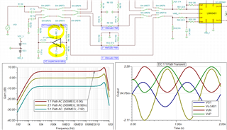
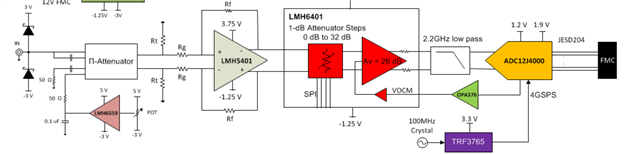
I have selected LMH5401 as my FDA before ADC(I wish to adopt TIDA-00826 reference design | TI.com )

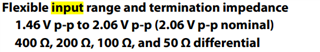
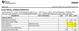
I have selected ADS5407 as my ADC

I wish to use the ADC for Both AC and DC coupling so i have given the option in my simulation for both and also given option of attenuation based on requriement.
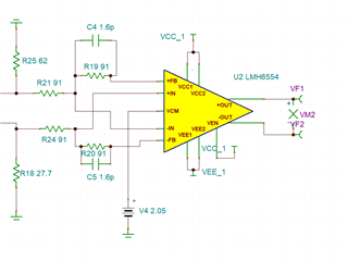
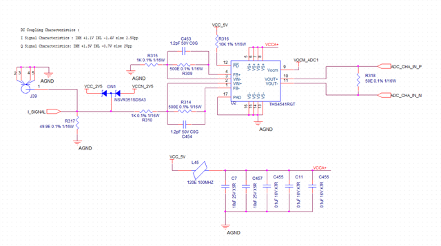
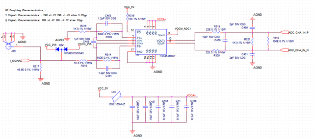
Below is my SCH

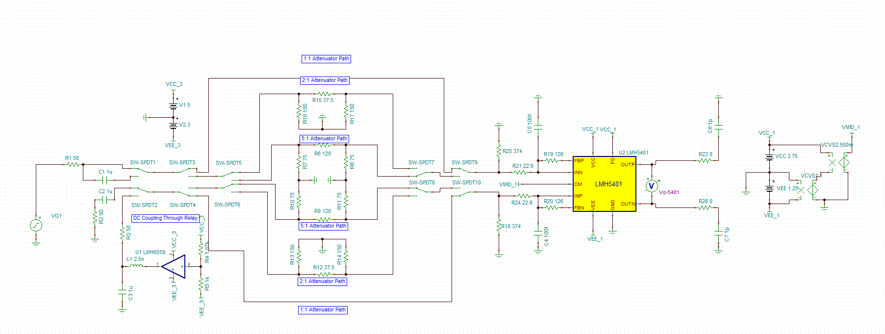
Attached also the TINA-Simulation-File

Kindly hlep me in understanding below

1. How to condition the Signal which is of below nature using the above circuitry to take to ADC

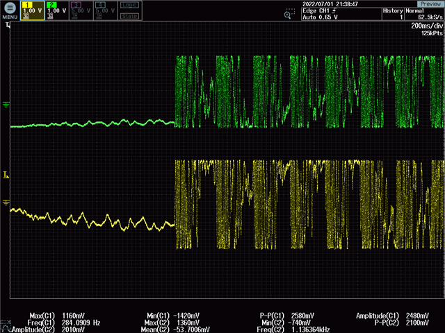
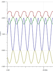
You can clearly see that my signal will have a DC shift in both channels, i wish to retain the DC shift because its a important parameter to measure, at the same time i also required to measure the AC variation in signal

At maximum the signal in Green Channel can touch +2V and Yellow Channel -2V

As taking this large swing to ADC is really tricky to me, high speed ADC i have seen will have swing of  2Vpp only

how to condition the signal to the ADC input

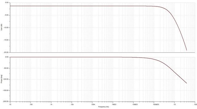
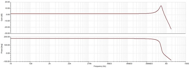
2. Why the simulation shows the plot of ADC gain negative that is less than 0dB ? am i doing wrong anywhere ? the fall 3dB/dec starts at 100Meg only why so ? i wish to operate the FDA up to 500Mhz with 1V/V Gain.

  • Hi Shyam,

    You need to ground the PD pin and run these again. You are getting erroneous results by simulating in power down mode.

    I'll keep looking and let you know if I find any other issues.

    Best,

    Sam 

  • You also swapped the supplies on you DC Coupler

  • Thanks for the help, it worked

    Now i wish to enter to details of op-amp suitablity

    i have understood my signal more and the activity recorded is below

    Q Channle is 2580mVpp and I channel is 2100mVpp

    i need to condition this signal to take it to a ADC and make full use of resolution of ADC

    Problem with existing Opamp is gain peaking at high frenquency,

    though my signal will not fall in the range, i feel there may be noise at high frequency which may get dominant , so i wish to tune the Opamp to frequency less than 500MHz strictly, after FDA i shall put one more LC Filter of 500MHz to filter much properly, i feel existing opamp tuning may require femto farad caps which may complicate and make design un-realisable.

    can i achieve above signal conditioning with LMH5401 ? or should i need to switch to Opamp like LMH6554  or less GBW opamp ? if so kindly suggest one with large Vpp which more or less 2.5Vpp

    as i dont need any gain but wish to convert input signal to differential only

  • Hi Shyam

    The LMH6554 is certainly a viable alternative, and we can also look at incorporating an active filter stage as well. I think the LMH5401 should still work fine but it might be a little overkill for this application. 

    Best,
    Sam

  • Hi i wish to use LMH6554 for attenuating my signal to half, i have my signal limits to 4Vpp in both channels so i wish to convert it to 2Vpp

    The input AFE will server for following purposes

    1.attenuation of 2:1 

    2.Single ended to Diff Conversion

    3. Filtering

    So Can you please suggest me the Rf,Rg,Rt values with Cf for serving above purposes.

    I hav experimented with a input of DC shift 1V and 200MHz 1Vpp sinusoid

    below values, but i have seen some issues in the output signal.

    Output signals

    I am not sure why signals are not that clean or proper in reconstruction.

    1. Kindly help me in selecting proper values of passives arround

    2. also i think as we are connecting the signal to inverting input the output is inverted and sent to ADC

    3. Can i give signal to non inverting end ? can it perform same ? wouldnt be same with every ADC front end, usually this is managed digitally ?

  • Hi Shyam,

    What is the power supply configuration in the simulation you have? Can you post the file? We can design a passive filter or an active MFB filter for you, is your -3dB target frequency 500MHz? Also is your sensor output 50 Ohm matched?

    Best,

    Sam

  • Attached is the spice simulation - LMH-6554  

    My RF output requires 50 Ohm Termination, so the input to LMH-6554 would be from a 49.9 Ohm Termination of course

    As my Vcm is 2.05 i assume i need to operate at +3.3 and -3.3 supply

    my inpu is maximum 200MHz, so i have picked a 500MSPS ADC

    Better if the signal is filtered to 200MHz and it should be attenuated by 50%.

  • Hi Shyam,

    For a only a 200MHz bandwidth I think we should look at the THS4541. I'm still a little confused about your specifications:

    - Is the input swing +/-1.8V or +/-2V? (both are stated above)

    - Is the input common mode 0V? (it is -200mV in your latest sim)

    - Is the input signal bandwidth 200MHz or 250MHz (both are stated above)

    - Are we still accounting for both the AC and DC paths and the multiple input attenuation networks (only 2:1 is specified)?

    We will need to be careful about stability/peaking when designing the FDA attenuator and also with the differential output offset since the ADC FSR is 1.25Vpp

    I just want to be sure we have everything correct here.

    Also be careful when using the source series 50 Ohm resistor in TINA, it is not like a matched real world source and will act as an voltage divider in front of the circuit. TINA does not handle RF reflections or mismatch, so you can just leave that out.

    Best,

    Sam


  • There are some different statments because in due course of time i have characterised the sensor practically.

    Final Requirements :

    1. Input swing is +/- 2V

    2. Input CM is 0V but due to the LO power given to the Optical - Electrical Mixer, there is a dc shift, also the signal nature from fiber causes dc shift,  which is why i wish to use DC coupling to preserve signal nature.

    3. Input Signal BW is Maximum 250MHz, i wish to experiment with 100, 150, 200 and 250, so with to keep the BW to maximum 250MHz

    4. I wish to do DC coupling only, i will place just 0Ohm resistor, when required i will replace it with a 0.1uF cap to make it AC coupling, spending on Relay is increasing my BOM cost

    5. I wish to make the AFE independent of ADC, because in future if based on BOM cost and final prototype after R&D i may change the ADC, so i will keep VCM of FDA in my control ranging from 1.25 to 2.05V, My ADC currently finalised is AD9684 and ADS5407.

  • Gentle Reminder, Can you please reply to the thread

  • Thank you for clarifying the specs, I'll have something for you later today.

  • Hi Shyam,

    Please see the attached files.

    Shyam Attenuator.TSCShyam Attenuator STAB.TSC

    Best,

    Sam

  • I have Few Major concerns with

    1.my input requirements as swing is +/- 2V, can a single supply of +5V handle the negative swing on non-inv terminal ? i am quite perplexed with this configuration

    Max Diff input voltage is +/-1V only, input voltage range is on negative side is Vs-0.5, which will be -500mv, but my input can swing up to -2V, kindly elucidate

    2. Can you please explain about the input and ouput capacitors of 10p you have placed, are they just for simulation needs ? should i need them in my actual schematic

    3. Kindly review my below final sch design, also kindly comment on the Protection diode chosen.

  • Hi Shyam,

    1. Please see: Using Single-Supply Fully Differential Amplifiers With Negative Input Voltages to Drive ADCs

    2. Input 1p increases high frequency noise gain to improve stability, output 10p is filtering.

    3. Your output here does not include any RC LPF so bandwidth is now ~275MHz, this diode's reverse voltage limit is only 5V, differential load matching for RF is usually 100 ohms

    Best,
    Sam

  • Thanks for the material reference, this has given me some idea of direction

    1. i have place the caps as suggested at input, and output, one of the adc i am intending use is having programmable input impdance option which is 50 ohm

    to avoid mis-match i have placed a 50 ohm output load resistance,am i doing wrong ? if i dont do so i may reduce the input range of ADC !

    Data sheet of ADC I am using : AD9684 (Rev. 0)

    2. I am using a 5V limiting because my input may not go beyond the limit of 5V both positive and negative side, i have pulled them to 2.5V postive and negative both sides, so that anything more than 2.5V should conduct up to limit 5V, any reason you are suggesting me to go beyond 5V ?

    3. As per my understanding  THS4541 should support up to maximum limit of Vs(+) - 1.2v which is 3.8, the output for a input votlage of 3.8V would be 1.9 which is with in the limit of ADC, so i assume the input limit through the diodes should not pose any problem to the FDA, kindly correct me if my understanding is wrong.

    After Summing up things my final design would be as below

  • Looks like 50 Ohm differential load is fine for that ADC.

    I'm not really following your diode logic. The intent is that if the input sees +2.7V, the top diode will start turn on to the positive rail, and if the input sees -2.7V, the bottom diode will turn on to the bottom rail. But for this diode, 5V is the reverse breakdown voltage. So you now have a situation where if the input goes to +2.5V the bottom side diode will start to breakdown before the topside diode turns on, so now the clipping diodes are likely operating in the reverse breakdown mode only... 

    Also, sorry for the confusion, the 1k load with the 2pF caps was just to model the input impedance of the ADS5407:

    You can remove those from the design.

    Best,

    Sam

  • 1. Diode Logic is adopted from 2Ghz Oscilloscope design, see the entry point diodes.

    how is it managed here ? 

    essentially i need to provide protection to FDA to avoid any damage to FDA, Kindly suggest some other way if the above way is not appropriate.

  • The implementation is fine but you need to choose diodes with a higher reverse breakdown voltage so that they are able to operate properly within those supply voltages.

    Best,

    Sam

  • I wish to share layout files to you, can you please accept my friend request

  • Please see your messages.

    Best,
    Sam