This thread has been locked.

If you have a related question, please click the "Ask a related question" button in the top right corner. The newly created question will be automatically linked to this question.

XTR117: XTR117 design check request

Part Number: XTR117
Other Parts Discussed in Thread: XTR116, , OPA2188, XTR111, TIDA-01536

Hello,

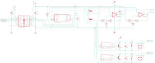
I'm building an isolated bipolar +-10V or current 4mA..20mA output module.

The voltage generator use an SPI isolator and 16 bit DAC.

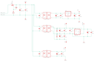
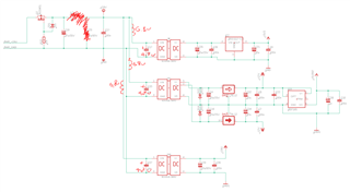
The power lines are:

  • 5V reference voltage (REF195)
  • +-12V
  • +24V

The output voltage works and it's been tested, it is based on the TI paper [SLAA869] Unipolar voltage output DAC to bipolar voltage output circuit.

The current output it's based on a commercial board, the MIKROE-1296.

Not sure if the output component and wiring diagram is correct, before building It i ask you a kindly check.

Also If possible, can you give me a hint on the power stage? That's based on the MORSUN 2W dc-dc modules.

Thanks!

  • Thank you, I've take a look to that post before writing this design, indeed there's some similarities.

  • Hi Davide,

    Not sure if the output component and wiring diagram is correct, before building It i ask you a kindly check.

    The selected components per the questions are identical to MIKROE-1296 EVM, and these components should work. 

    Also If possible, can you give me a hint on the power stage?

    I am going to briefly explain what power stage around XTR116/XTR117 4-20mA transmitter. Please read the link suggested by Kai, and you may check the power connection in details. It is not clear how XTR117 is powered and referenced from your schematics. 

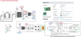
    Here are some highlights based on the EVM. 

    a. Green box is shown where the EVM's input Vloop is located, which is reference to GND. 

    b. Vcc_iso is V+ inupt signal from Vloop power source, shown in marked Red oval.

    c. GND_iso is Iret or pin3 of XTR117, which is a floating ground, shown in Torquoise oval

    d. Vref and Vreg or pin8 are floating 5Vdc that is regulated by XTR117 (shown in dark blue oval); its floating reference is Iret or pin3. FYI, Vreg is only able to source approx. @5Vdc vs. Iret pin at 3.5mA range. 

    MORSUN 2W dc-dc modules will work for the project, but I will need to see your overall block diagram in order to comment on it. It seems that your schematic deviates from the EVM's wiring connections and I need to know the reasons. 

    Enclosed are V-to-I, 4-20mA transmitter links, in case you are interested. 

     https://e2e.ti.com/support/amplifiers-group/amplifiers/f/amplifiers-forum/945188/faq-designing-with-4-20ma-current-loop-transmitters-xtrs-faq-links

    Best,

    Raymond

  • Thank you!
    I know, my schematic is not so clear.

    But i can confirm you it's like the MIKROE-1296 EVM, which is my reference design.

    a. EVM input is located at AOUTC1-1 and AOUTC2-1, after the rectifier, like the image you post

    b. V+ is connected to +24V supplied by the bottom DC-DC of my schematic

    c. Iret is connected to the GND of the bottom DC-DC

    d. Vreg is not connected. I use REF195 to provide reference 5V for the my DAC (AD5663), the isolator (ADUM1401), Vref of XTR117, and reference for +-10V stage for voltage output (OPA2188)

    Furthermore, about the grounding. The GND between the +24V DC-DC converter and +-12V DC-DC converter and +5V ref is connected.
    This ground point MAY BE connected to Earth, cause it may happen that devices driven by the voltage output has ground connected to Earth.

    So I've a couple of new questions:

    1) Could be a problem if GND point of Iret is not connected to Earth?

    2) I've added Rin to my design. Does 20k fit for my 0 to 5V output AD5663?

    Thanks!

  • Hi Davide,

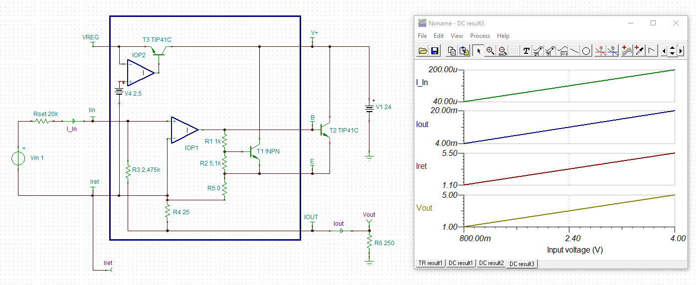
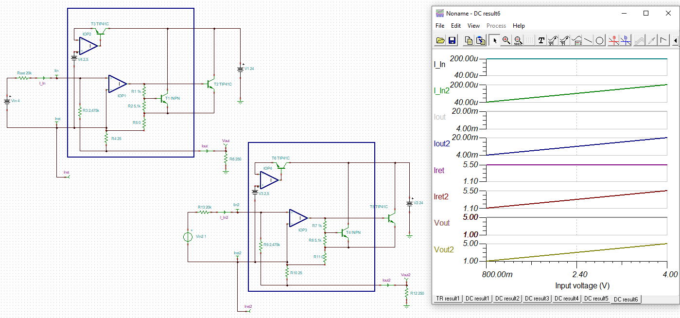
    you must not connect the both "Iret" pins of the both XTR117 together. "Iret" floats and changes its potential according to the input signal. Because of this "Iret" must not be used as ground pin:

    davide_xtr117.TSC

    Not only "Iret" is floating, by the way, but also the whole input signal "Vin" and the whole input circuitry driving "Vin".

    If your both XTR117 see different input voltages, then the individual "Iret" will have different potentials. When shorting them together, the XTR117 will no longer work:

    davide_xtr117_1.TSC

    In the above simulation the input signal of the left XTR117 is 4V while the input signal of the right XTR117 is varying from 0.8V to 4V.

    See how the potentials of "Iret" and "Iret2" are moving against each other. You must allow them to freely float against each other.

    Kai 

  • Get it,
    I also take a look here: https://e2e.ti.com/support/amplifiers-group/amplifiers/f/amplifiers-forum/840887/xtr117-two-xtr117-with-acceptable-error
    The only way would be isolate my Iref. I've to think if it isn't simpler for my design to use an op-amp as current source.

  • Hi Davide,

    have you thought about using the XTR111?

    Kai

  • Not yet!
    Thanks for suggestion, I'll give it a try.

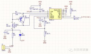
    I found the implementation below, is that a good design to be attached to my power lines?

  • Hi Davide, 

    Thanks for Kai's simulations and suggestions!

    Please let us know if you have additional questions. 

    Best,

    Raymond

  • Hi Davide,

    the EVM User's Guide shows a suited circuit:

    sbou048c.pdf

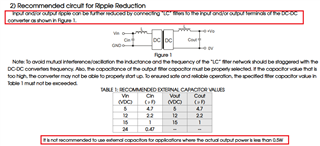
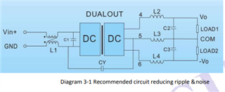
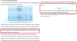
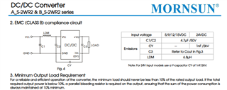
    There's another issue: DC/DC switchers like your MORNSUN thingy produce extremely high ripple noise at the input and output which can totally ruin the performance of an analog cicruit. The datasheet mentions an output ripple of 200mVpp up to 20MHz. This is quite a lot. So I highly recommend to use Pi-filters at the input and outputs. Pi-filters have already been discussed here:

    https://e2e.ti.com/support/power-management-group/power-management/f/power-management-forum/669266/lm3940-pcb-layout-and-capacitor-selection

    https://e2e.ti.com/support/power-management-group/power-management/f/power-management-forum/687264/tps7a83a-maximam-capacitance

    https://e2e.ti.com/support/amplifiers-group/amplifiers/f/amplifiers-forum/707560/ina126-ina126-output-unstable-at-gain-368

    https://e2e.ti.com/support/audio-group/audio/f/audio-forum/716707/drv135-high-frequency-11-4-khz-noise-issue

    Kai

  • Hi Davide, 

    Kai has provided you with the additional design references and suggestions. 

    If you have additional questions, please let us know. 

    Best,

    Raymond

  • Thank you all,

    I'm looking further in the XTR111 direction, vs use of an op-amp.

    As for the MORSUN, really thanks!
    I'm going to use the 24V to +-15V and add a +-12V regulator, this should attenuate the output ripple.

    Wondering if the 24V used for the current output loop can have ripple, or should be cleared it too.

  • Hi Davide, 

    I do not know how the DC-DC converter will perform under certain load over frequency (the BW of noise ripple is fairly wide up to 20MHz). Please use LC filters to reduce the noise ripple, if it is not acceptable under a given load. 

    Alternatively, you may use similar circuit to reduce input ripple voltage as shown below. You may use power NPN transistors or power Darlington NPN to replace 2N2222A, if the load current is high. Or you may use another low noise LDO after the DC-DC converter. I'd try the method suggested by the manufacture first. 

    Note: the alternative method would work, but you will dissipate additional power in order to exchange for lower ripple voltage power source for XTR111. 

    Reduce Ripple Noise 07112022.TSC

    Wondering if the 24V used for the current output loop can have ripple, or should be cleared it too.

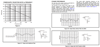
    XTR111's PSRR is approx. at 120dB range at 10Hz. If you are able to filter out input ripple voltage noise above 1kHz range, the application should have good V-to-I 4-20mA current loop conversion, where the current ripple should not be a concern. 

    If you have additional questions, please let us know. 

    Best,

    Raymond

  • All clear! Thanks!

    Now I'm working an embedded software for another board, as soon as I get back to this board I'll let you know progress.

  • Hi Davide,

    I would like to encourage you to use pi-filters at the inputs and outputs of DC/DC switchers in any case. Not only because many LDO have a very limited ripple rejection at higher frequencies, but also to prevent the switching noise from spreading over the whole circuit and contaminating your application with EMI. And if any cabling is involved, even the least remaining switching ripple on the cable can make your application fail the CE testings.

    So stop the switching noise from the scratch by mounting pi-filtes directly at the inputs and outputs of all DC/DC switchers you have. "Directly" means that the ground terminals of filter caps and the ground terminals of switcher should have the shortest distance ever possible.

    And if you have an isolated switcher, install an Y-cap closest between the input and output ground of switcher. Every millimeter counts! Because lowest impedance at the switching harmonics is extremely important here, I always mount two or even three identical Y-caps in parallel. And if no isolation is needed in an application, I connect the two grounds by a low impedant ground connection. This gives you a way better feel when doing the CE testings Relaxed

    In the todays world with its harsh EMI regulations a DC/DC switcher must always have state-of-the-art filtering by using optimized pi-filters at the input and output(s) and by using an optimized Y-cap between the isolated grounds.

    Kai

  • Thanks for this feedback.
    I've added +-12V regulator after a DC-DC 24 to +-15V.

    Also I've added a pi-filter, 47uF + 6.8uH + 10uF on the main input.
    I'm going to build it on a breadboard and check ripples.

    +3V3 is for the microcontroller

    +-12V for the voltage output
    +5V REF is the reference voltage for the DAC

    +24V is for the current output (which I'm also working on)

    The purpose of this board is to read values from and encoder, and covert it to voltage or current regarding the setup found in the main microcontroller (STM32).

    I hope just one pi-filter on main input is enough.
    I'm more an software person than a electronic eng. So excuse me if may questions are dump. Also my reply are so late cose I've other project going on.

  • Hi Davide,

    your questions aren't dump at all Relaxed

    I hope just one pi-filter on main input is enough.

    Even if you don't want to here it, from my experience I can only suggest to use a pi-filter directly at the input and the output of each switcher. It depends a bit on your application: If you have to pass these many nasty CE testings I would not omit any of these pi-filters. Especially if any cabling is involved.

    Aluminium electrolytic capacitors are ideal for the pi-filter. The ESR of these caps can very effectively help to prevent the ringing of LC filter. Just use caps with standard ESR. Low ESR types are less suited.

    Kai

  • Thanks! I'm going on vacation today, I'll post any further update here.

  • Hi Davide, 

    I am going to close the inquiry for now. You are still able to post questions in this thread or you may also open a new one. Enjoy your holiday!

    Thanks Kai for all the help! 

    Best,

    Raymond

  • No problem, I can not click on just 1 reply "This resolve my issue", cause more than one solve my issue.
    Thanks!

  • Hello,

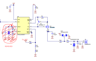
    I've take as reference the design of the TIDA-01536 board.

    I don´t need a regulated 5V output, so I will not connect output for pin REGF, REGS. 5V_REF for SET pin from my power supply stage. +24V from my supply stage. GND is common between 5V_REF and 24V.

    As for circuit protection and output, wondering if the following component are a good replacement cause I can not find the same as proposed in reference schematic:

    A- Q2: NTR5105PT1G, p channel 60V, 211mA. Shouldn't this be enough for the 40mA output?
    B- D2A: Semiware SESR70

    today I've review the supply according to your suggestions and the values suggested on mornsun datasheet for the  A_S-2WR2 and B_S-2WR2 series.

    Removed the main Pi-filter, added a filter for each DC DC converter. I'm not using the Y cap filter.

    My question on this supply stage is:

    1- what type of inductor have i to use? can i use a ferrite type SMD inductor of 500mA like the CMP321609XD6R8MT? or have i to use power inductor like the YNR3012 750mA rated? I think something < 400mA would do the job. R ight?

    2- wondering if the dual regulator +-12 are needed or I can go straight on from the DC DC regulator to the op-amp voltage conditioner you can find in first post


    Note: excuse the crudity of the attached schematic, I'm on vacation with reduced software resources.

    Thanks again.

  • Hi Davide,

    1- what type of inductor have i to use?

    I would like to encourage you to use pi-filters at the inputs and outputs of DC/DC switchers in any case.

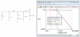
    Since REG117-3 has a reasonable ripple rejection up to 60+dB range at 1kHz, it will be the effective to design a LC cutoff frequency at 10kHz or lower (the switching frequency of DC/DC converter is approx. 100kHz). 

    For the 24Vdc DC/DC regulator, you may try the following. You need to calculate what is the saturation current in an inductor. Assume you are using 68uH inductor as shown above. 

    BTW, you will need to use low ESR ceramic capacitors at the output of DC-DC regulator in order to lower your ripple output voltage. 

    E2E Pi Filter 07182022.TSC

    2- wondering if the dual regulator +-12 are needed or I can go straight on from the DC DC regulator to the op-amp voltage conditioner you can find in first post

    I do not know how noisy these DC-DC conveters actually are. If you want to reduce the noise further in ±12Vdc supply rails, you may need to use a common mode filters at the output of ±12Vdc DC-DC converter. The technique is similar to the simulation, which the output may require to be dampened in order to reduce the Q effect. 

    If you have additional questions, please let me know. 

    Best,

    Raymond

  • Thanks Raymond.
    I get now the point on 1), the relation with ripple rejection I mean.
    About the inductor type, for this kind of application can I use multilayer chip inductors or it's better to use shielded power inductors?

  • Hi Davide, 

    Passive Components 6.8uH 20% 500mA 1206 CMP321609XD6R8MT For Inductors

    Could you send me the datasheet for the multilayer chip inductor? 

    I do not know how much current that each DC/DC converter is operating in actual circuit. Assumed the nominal current is approx. 100mA for 24Vdc power rail, the saturation current of the inductor has to be greater than this DC operating current in order to avoid magnetic core saturation. In addition, the purpose of pi filter is to lower the cufoff frequency of LC filter from DC/DC converter, which is to attenuate higher frequency noise.  The application is targeting the LC resonance frequency near 10kHz range, which f = 1/(2*pi*sqrt(LC) is the equation. If you use small L, then you need large C to generate a desired LPF. 

    it's better to use shielded power inductors?

    My guess is that the DC/DC converter is generating higher level of electrical and magnetic interference than the pi filter. I would be more concerned about the conducted emissions from the DC/DC converters than using the shielded power inductors. 

    You uses three DC/DC converters to generate 24Vdc, +/-12Vdc, 5Vdc and 3.3Vdc per the design from a 24Vdc source. Can you tell me the purposes? I would invest higher quality of a single DC/DC converter, say 24VDC --> +/-12Vdc, then convert the remaining voltage rails from +12Vdc --> 5.0V and 3.3Vdc using linear LDO and high efficient switching converter.  If the current requirement is low for the application, I would use linear LDO to generate 5Vdc and 3.3Vdc on board from 12Vdc. I need to know more about your application. 

    Best.

    Raymond

  • Thanks.

    I can find only in chinese : https://datasheet.lcsc.com/lcsc/1912111437_FH-Guangdong-Fenghua-Advanced-Tech-CMP321609XD6R8MT_C395031.pdf

    I'm building a board that convert output for encoders. 2 encoders with each one his output.

    The output are digital SPI (my board is a slave) AND voltage (+-10V) OR current (4..20mA) jumper selectable.

    Input are isolated by using optocouplers.

    Output must be isolated.

    So, +3.3V line is the microcontroller one, that needs to be isolated from the output and inputs.

    Output lines are voltage +-10V and current (4..20mA). They need to be isolated. Output for the 2 channels can have common ground. +-10V lines are obtain centering the 5V output from DAC using an op-amp supplied with +-12V. For the 2 current output I would like to use 2 XTR111 and the +24 line. +24 and +-12V have common ground.

    On first page you can find the schematic (do not consider the XTR117).

    The actual board works but the power lines differs. It has +-12V and +12V line. I would like to make just one line (+24V) and get all output from this line.

    Two input and output channels are implemented for 2 encoders.

  • Hi Davide, 

    Thanks for the datasheet. 

    It looks like different 2520 TYPE or 3216 TYPE are different magnetic materials and dopant in the multi layer chip inductor. I think that Ir refers to the maximum rated current. I am looking for Saturation current, where the magnetic filed no longer increases proportionally with an increasing current (which I do not see from the pdf file). 

    I will search the company's website and see if I am able to find additional tables, graphs about the multilayer chip inductors. Please let me know what is the nominal current you are operating in each of power line. That will help to select the types of inductors. 

     I would like to make just one line (+24V) and get all output from this line.

    This will give you PWR_GND = GND and COM, where COM = GND1 is your isolated ground. Is this what you have in mind? 

    Please see the following section of the DC/DC design consideration for the converter. 

    https://www.mornsun-power.com/public/uploads/enfiles/mornsun_fixed_input_voltage_dc-dc_converter_application_guide_2021.pdf

    Best,

    Raymond

  • Thanks Raymond,
    for my board GND must be isolated from COM ground, and also the microcontroller ground itś better if is isolated, cause there's also a UART output to the PC (the one which came from the 3.3 regulator).

    As for the inductors, I'll use power inductors, think it's better than those multi layer chip.

    +3.3V line current (microcontroller + optocoupler output + cp2102 + led) will be something like  100mA

    +-12V line and + 5V_REG (isolator + DAC + opamp), i think 20mA

    I would like to keep PWR_GND isolated from all the other ground, so isolated from COM = GND1.

    Maybe I can save the 24 to 24 DC DC converter using a step up converter 12V to 24V, min 100mA (for both current output). Have to think about this.

    I'll measure ripple as soon as I get components for testing.

    On datasheet they use a simpler approach, ripple will be reduced less, but for my board maybe it will be enough.

    I'm using the filter proposed here: https://www.mornsun-power.com/html/pdf/B0505S-2WR2.html

    About my TIDA-01536 questions (my 3 days ago reply), do you think A and B components will fit?

    Thank you!

  • Hi Davide,

    As for the inductors, I'll use power inductors, think it's better than those multi layer chip.

    Power inductor is what I would suggest from the get go. You may use multi-layer chip inductors, if it is for low current and power in switching application, but I do not see the full specification from the datasheet. In the power supply switching application, the inductor's core will get magnetic reset in each cycle. Since you are using the inductors for DC ripple LP filters (with DC current component + AC ripple peak current), you need take into account of an inductor's saturation current and ripple voltage from DC/DC converter. The selected inductors per the application shall not be operated under a magnetic core saturation  in any operating conditions and temperature. 

    +3.3V line current (microcontroller + optocoupler output + cp2102 + led) will be something like  100mA

    Since the LC filter has nominal current of 100mAdc, say 50mV ripple up to 100kHz, I would select an inductor (low ESL) with saturation current rated between 0.2Adc to 0.3Adc, say 0.25Adc. Typically, I would provide 2X to 3X current margins so that the inductor's will not go into core saturation over a temperature. 

    The LC resonance frequency equation is posted previously. Say if you are using 22uH with Isat = 250mA inductor, with the LC cutoff frequency of 5kHz, the calculated capacitance needs to be 47uH, low ESR, ceramic capacitor. You may require to dampen the LC filter to lower Q of the filter, see the simulation that I posted previously. 

    From the above inductor selection guide lines, you may pick other inductors as well. Please follow the manufacture's application notes FYI. You mentioned that you are going to test the noise, ripple and other DC parameters, you may then improve the design once the PCB is populated.  

    When you characterize the noise and ripple voltage from DC/DC converters, please use the short ground tip + probe, so that you do not have to pick up unwanted switching noises. Play around shielding from the DC/DC converters, if you want to achieve low noise in the design application.  

    A- Q2: NTR5105PT1G, p channel 60V, 211mA. Shouldn't this be enough for the 40mA output?

    I may beef up the Q1 slightly. It is power dissipation that I am concerned about. Say 24Vdc*20mA = 0.48W (it is a bit high for SOT23 package),  which is higher than  NTR5105PT1G can handle. Below is the recommended BOM, which it can be found in the TIDA-01536 link. 


    B- D2A: Semiware SESR70

    This is fine. 

    If you have additional questions, please let me know. 

    Best,

    Raymond

  • Thanks! all clear now.
    I'll post here updates as soon as I've build prototypes.