This thread has been locked.

If you have a related question, please click the "Ask a related question" button in the top right corner. The newly created question will be automatically linked to this question.

TLV9304: Design Verification for 0-10V & ±10V Output

Part Number: TLV9304
Other Parts Discussed in Thread: DAC128S085, TLV9302, , TLV4172, OPA4191

Hai Sir,

My End application is - Controlling & Analog outputs driving.

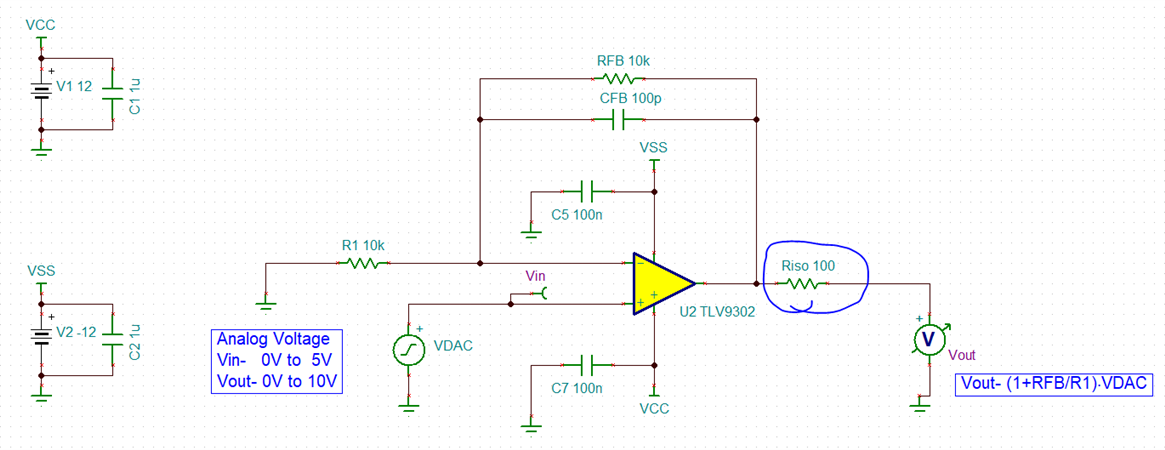
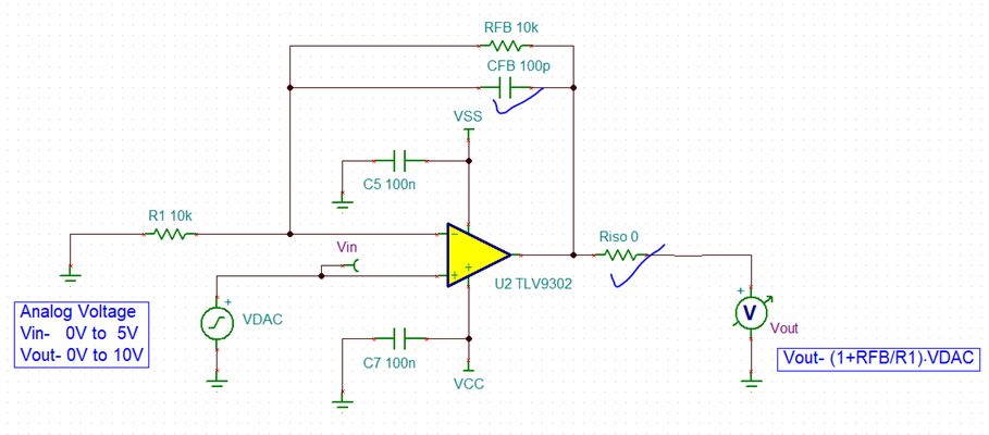
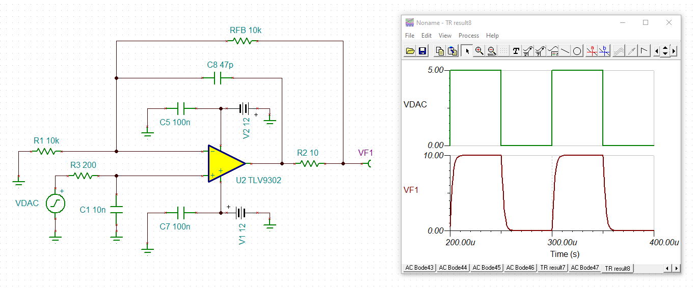
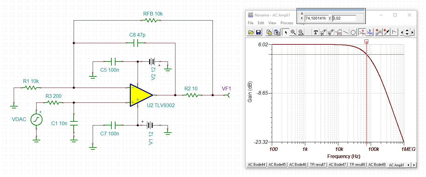
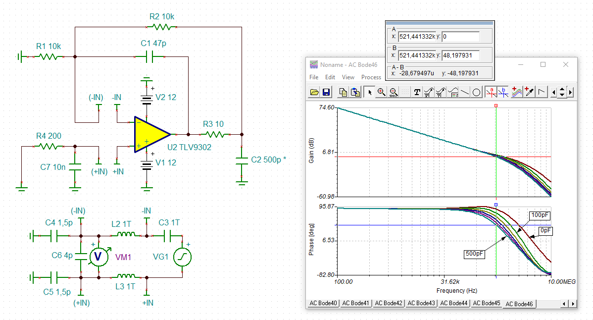
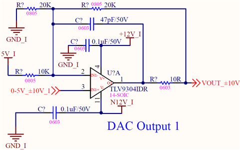
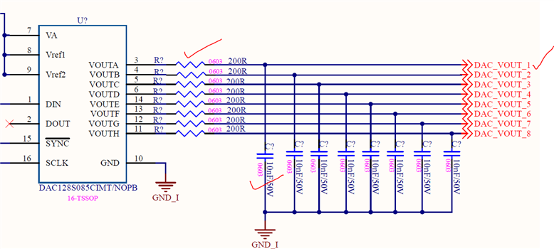
We are planning to generate the 0-10V & ±10V output using Opamp-TLV9304. Here we have to give the input voltage(0-5V) to Opamp is from DAC (DAC128S085).

Can you please verify the attached tina simulation file for design verification to generate 0-10V & ±10V from 0-5V and let me know if any modifications to be done.

0-10V & ±10V_OpmapTLV9304.09.08.22.TSC

  • Hi,

    why have you chosen the dual feedback topology? To make the circuit immune against capacitive loads?

    Keep in mind that the dual feedback topology only works properly for a somewhat limited load capacitance range:

    sandeep_tlv9302.TSC

    A remedy to narrow this range is to add a dummy capacitance to the output. This has many other benefits: It helps to absorb ESD and EMI coming from outside and it helps to limit the signal bandwidth by low pass filtering.

    Kai 

  • why have you chosen the dual feedback topology?

    It means Both Resistance & capacitance feedback. 

    To make the circuit immune against capacitive loads?

    Yes sir.

    Actually i referred this circuit from the attached design 

    https://www.ti.com/tool/TIPD125?keyMatch=&tisearch=search-everything&usecase=refdesign

    Can i use this design without feedback capacitance...for generating the 0-10V & ±10V output. or keep it same design.

  • Hi M Sandeep,

    Can i use this design without feedback capacitance...for generating the 0-10V & ±10V output. or keep it same design.

    This sounds like using the Riso method where you just have an isolation resistor. We have some collateral on this which can be found here: Stability: Isolation Resistor, where it goes over the advantages and disadvantage of using just an isolation resistor and the method you are using, Riso + dual feedback. Both of these methods of isolating the op-amp from the capacitive load have advantages and disadvantages. 

    Do you know what the expected output capacitance the op-amp will see? That could help you determine which isolation topology works best for your needs.

    Best Regards,

    Robert Clifton 

  • No sir....I don't know the how much of the capacitive load .....i have only requirement of generating 0-10v and +/-10v....

    If any disadvantages occur with this Riso resistance and feedback capacitance....can I remove those parts.

  • Hi,

    Actually i referred this circuit from the attached design

    Yes, but you have made a lot of changes. You use a different OPAmp and you removed the cap from the output to signal ground. By this you have a totally different circuit.

    Without a big load capacitance at the output of OPAmp you don't need the dual feedback method as discussed here:

    https://training.ti.com/ti-precision-labs-op-amps-stability-isolation-resistor?context=1139747-1139745-14685-1138805-13953

    Then make Riso=0 or move it outside the feedback loop, if you need a current limiting resistor at the output. This current limiting resistor can also serve as isolation resistor against moderate capacitive loads.

    The 100p cap in the feedback loop can stay in the circuit because it provides a phase lead compensation and will improve the phase margin. All my circuits have such a phase lead capacitance in the feedback loop. It also limits the bandwidth, improves the noise performance and provides some low pass filtering of the glitching noise eventually coming from the DAC.

    Kai

  • Then make Riso=0 or move it outside the feedback loop, if you need a current limiting resistor at the output. This current limiting resistor can also serve as isolation resistor against moderate capacitive loads.

    The 100p cap in the feedback loop can stay in the circuit because it provides a phase lead compensation and will improve the phase margin

    Yes sir... i understood from reference video link about dual feedback advantages & disadvantages...

    I have required only resistive and moderate capacitive loads only. So, As per your suggestion, i made the design, pls verify once...

    i keep it CFB feedback capacitor and i moved the Riso resistor from feedback loop and is it required the Cload capacitor in the main circuit.

  • Hi,

    when you do it this way, then the 1n cap at the output should be removed.

    Keep in mind that the 100R resistor at the output will cause a voltage drop in combination with the load resistance (= input resistance of following circuit) now. So the output voltage will be lower than planned. Is this ok? If not, you would need to decrease Riso.

    By the way, the dual feedback method does not suffer from this issue, because the voltage drop across Riso would be fully compensated then.

    Kai

  • when you do it this way, then the 1n cap at the output should be removed.

    Ok sir... i'll remove this..

    Keep in mind that the 100R resistor at the output will cause a voltage drop in combination with the load resistance (= input resistance of following circuit) now. So the output voltage will be lower than planned. Is this ok? If not, you would need to decrease Riso.

    No sir.. i required 0-10V exactly.

  • Hi M Sandeep,

    If you require exactly 0-10V then the dual feedback method is likely the best option for you to avoid the voltage drop. If there's some flexibility, then you could lower the Riso resistance to minimize the voltage drop across from it. 

    What exactly is the op-amp driving? Many components capacitances can be found in the datasheet to help derive what cap load the op-amp will see. This might also help you figure out whether or not any Riso is necessary. 

    Best Regards,

    Robert Clifton 

  • Hi sir..

    Presently we are planning for Resistive loads only as per customer reference....

  • Hi,

    yes, but when you use a cable then you have to struggle with the cable capacitance.

    What exactly is connected to the output of TLV9302? What is the load capacitance range? What is the load resistance range? Is a cable connected to the output of TLV9302? If yes, up to what length?

    Kai

  • Hai sir,

    What exactly is connected to the output of TLV9302? What is the load capacitance range? What is the load resistance range? Is a cable connected to the output of TLV9302? If yes, up to what length?

    As per clarification with customer. They will connect the resistive type loads only like PLC and Gain amplifiers. And also they will use the normal wires for connecting the loads. Length also normal range.

    1) 0-5V to 0-10V Design

    2) 0-5V to ±10V Design

    3) In both designs i'll reduce the Riso resistance to 10ohms or 0ohms

    So, Can i use these designs for further process?. or Can i use the Dual feedback design with making the Riso to smaller resistance

  • Hi,

    And also they will use the normal wires for connecting the loads. Length also normal rang

    What is "normal wires" and what is "normal length"? Is 1m 50R coax cable a "normal wire" and "normal length"? Such a cable can show 100pF and already present a problem.

    It all depends on the load capacitance seen by the output of OPAmp. This decides how to proceed.

    3) In both designs i'll reduce the Riso resistance to 10ohms or 0ohms

    If the load resistance is 1k, 10R presents an error of 1%. If the load resistance is 10k the error will be 0.1%. So, again, how to proceed depends on the load resistance and the allowed error, which we do not know.

    So, Can i use these designs for further process?

    I cannot answer this question without knowing the maximum load capacitance and the minimum load resistance.

    Kai

  • Presently, no information from customer about Loads. They are mentioning only the loads are PLC modules.

    So, Presently as per standard design of non inverting, i'm going with Single feedback network with compensated feedback capacitor and placing the Riso resistance to 0ohms. Based on Practical verification i'll change the Riso Resistane.

    If any changes pls let me know. Thank you for your support...

  • Hi Sandeep,

    ok, then I would do it this way:

    sandeep_tlv9302_2.TSC

    This circuit will properly work with load capacitances of up to 200pF and will be stable with load capacitances up to 500pF. This even allows the connection of a short cable:

    sandeep_tlv9302_3.TSC

    (Do not connect C2 to the circuit. C2 only represents the unwanted load capacitance of cable or PLC input.)

    By the way, the 200R and 10nF components are recommended low pass filters at the output of DAC. See the "EVM User's guide".

    Kai

  • Hi M Sandeep, 

    I agree with keeping a place to put an Riso value in case it's needed. It's difficult to know whether or not you will need the Riso without knowing what the maximum load capacitance is. 

    I've got no further comments from my end! 

    Best Regards, 

    Robert Clifton 

  • Hi Sir,

    Thank you for your reply,

    1) Ok sir...I'll proceed with this design for both 0-10V & ±10V outputs...i am attaching the modified designs.

    a) 0-10V Output

    b) ±10V Output

    c) DAC Outputs filter section

    By the way, the 200R and 10nF components are recommended low pass filters at the output of DAC. See the "EVM User's guide".

    2) Yes sir....i already placed the low pass filter circuit at DAC outputs in my design. That's why i am not placing these components at Opamp input.. Pls see the attached image for DAC outputs.

    3) And here i am using the TLV9304 for Quad channel purpose. In future if stock is not available for this component, i am suggesting the alternate part numbers to customer are TLV4172 or OPA4191. Are they ok for this 0-10V & ±10V design?

  • Hi Sandeep,

    the schematics look good.

    3) And here i am using the TLV9304 for Quad channel purpose. In future if stock is not available for this component, i am suggesting the alternate part numbers to customer are TLV4172 or OPA4191. Are they ok for this 0-10V & ±10V design?

    You can carry out exactly the same simulations with the alternative OPAmps as I did with the TLV9302 to see whether they are suited or not Relaxed

    Kai

  • Ok thank you sir...