This thread has been locked.

If you have a related question, please click the "Ask a related question" button in the top right corner. The newly created question will be automatically linked to this question.

OPA189: Improper step response of OPA189 based low side noninverting photo diode amplifier

Genius 15639 points
Part Number: OPA189
Other Parts Discussed in Thread: LM7705, TINA-TI, OPA182, OPA192, LM2674

Hi Experts,

Good day. Seeking you assistance on this:

I have used OPA189 for amplifying photo diode voltage using a non-inverting amplifier configuration. I did not use a traditional TIA configuration as I am using single supply and output must be zero in dark. the device is used for display panel characteristic measurement.

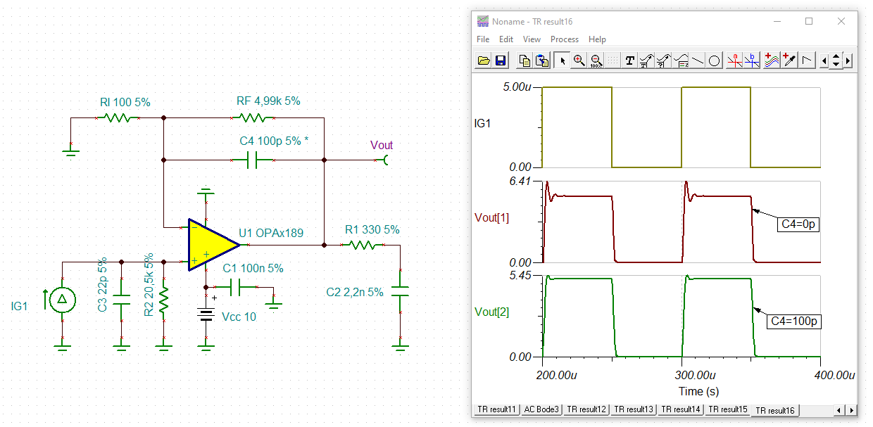
When I tested the circuit under any pulsing light (e.g. a display panel which does PWM dimming), I see the step response is not correct. Please refer the attached image. This problem happens only when supply voltage is > 5.5V. I tested the light sources through other sensors and confirmed that the sources generate proper square wave. I got a good square wave even with this circuit, if the supply voltage <= 5v. I also tested the input to the noninverting input to confirm the distortion is not present at input. I have also used DC battery and different kind of power supply modules to eliminate any power related issue. Issue happens with lower Opamp gain as well.

Please let me know what could be the possible reason for the issue and possible solution.

For your assistance. Thank you.

Regards,
Archie A.

  • Hi Archie,

    I did not use a traditional TIA configuration as I am using single supply and output must be zero in dark.

    This can very easily be overcome by using the LM7705 at the negative supply voltage pin. The LM7705 generates a negative auxiliary supply voltage of -0.232V and was designed for exactly these applications.

    It's not quite clear to me why the output of OPA189 is limited to 1.5V. But when running a TINA-TI simulation it can be seen that the circuit is not very stable. I would mount a phase lead capacitance of 100p in parallel to RF and see if it helps:

    archie_opa189.TSC

    Can you scope the output of OPA189? Also when having the ADC disconnected from the output of OPA189?

    Kai

  • Hello ArTzy,

    Adding to Kai's sage advice regarding your OPA189 photodiode TIA circuit do be aware that op amps using a periodic autocalibration technique to provide low input offset voltage and very low input offset voltage drift can have a different output recovery characteristics than conventional (non-switched signal path) op amps.

    When the OPA189 is driven to the negative output rail (Vo) which is the case when the photodiode isn't producing any current, the two inputs are separated by a voltage difference about equal to Vo. The op amp sees this large voltage as an offset voltage and attempts to autocalibrate it to zero. Then, when the photodiode does start producing current again and the output starts moving off Vo the OPA189 processes the changing offset value. It goes through a recovery phase until the offset is back within the normal range. Kai's suggesting of adding the LM7705 -0.232 V charge pump at V- keeps the output near zero, away from the Vo rail.

    The OPA189 is a very complex op amp with its autocalibrate, Mux-friendly and slew boost features. The square wave perturbance on the positive edge between about 1.3 and 1.5 V looks like it might be related to the slew boost circuitry behavior internal to the OPA189. For slew boosted op amps the slew is maximum for most of the square wave transition from low to high, but as it approaches the maximum voltage the slew slows to reduce overshoot. It could be the slew boost behaves differently with a single supply of +4.5 to +5.5 V, than it does with a a supply > +5.5 V. 

    See below for more information about slew boost:

    https://training.ti.com/sites/default/files/docs/opamps-slew-rate-introduction-presentation-quiz.pdf

    It would be interesting to see if the square wave, positive edge perturbance changes if you do employ the LM7705 at V-.

    Regards, Thomas

    Precision Amplifiers Applications Engineering

  • I do think the distortion of the square waveform has to do with OPA189 chopper amplifier trying to auto-correct a large input offset voltage after it was induced by the output being pushed against its negative supply.  To confirm, please use instead a linear RRIO op amp like OPA192, or try a latest zero-drift OPA182 that may be more forgiving.  Having said that, the best approach would be to use LM7705 Kai suggested to power (V-) with -230mV, thus, eliminating the non-linearity of the output stage all together.

  • Hi Team,

    Thanks for your detailed explanation.

    Trying the LM7705 but that increases noise in the circuit. Customers needed a very low noise circuit.

    What about LM7709? It meets most of my requirements too. Do you think even that will have such nonlinearity?

    Rgards,
    Archie A.

  • Hi Archie,

    Trying the LM7705 but that increases noise in the circuit.

    The LM7705 doesn't increase the noise when being decoupled and filtered properly. As an example: I have a circuit being powered by the LM2674 switcher amplifying 100nV signals and the noise isn't increased because of clever filtering with the todays ferrite beads and ceramic high caps.

    I did not use a traditional TIA configuration as I am using single supply and output must be zero in dark.

    If you say that the output must be zero in dark, then you must have a negative supply voltage to prevent output saturation of OPAmp. And if you don't want to use the LM7705 then you need to generate the negative supply voltage in another way.

    If the output must not be zero in dark, on the other hand, you can use a classic TIA with added DC shift (pseudoground) at the +input as shown in this appnote:

    8407.tidu535.pdf

    Kai

  • Archie,

    Agreed with Kai here, we have seen the LM7705 successfully adopted in many systems.

    Regards,
    Mike

  • Thanks, Michael, Kai.

    I need the output to be ZERO in dark. I also don't have margin to accommodate DC shift. I need full 0-10V range mapped to 0 - xxx optical brightness. Hence classic TIA or DC shift circuits will not work. LM7705 is a viable option, if the noise is below 1 mV.

    Can you share the LM7705 circuit you mentioned that has very low noise?

    Regards,
    Archie A.

  • Hi Archie,

    here's a nice appnote:

    sbaa373.pdf

    Kai

  • Hello ArTzy,

    Even if a photodiode is placed in a completely dark environment it will generate a very small dark current due to thermal agitation. The dark current is a tiny fraction of the current level compared to the current produced when the photodiode is irradiated by light. I show as an example the photocurrent and dark current curves for for the BPW34 photodiode are seen here. The vertical scale in Fig. 3 is 1000x that of Fig. 1.

    We can see that for this diode the dark current is about 2 nA at 25 C in Fig 1. The dark current would contribute about 40 uV of additional offset when it flows through the 20.5 kilohm resistor.

    There is a way to somewhat compensate for the photodiode dark current using a differential photodiode circuit. It relies on matching two of the same type photodiodes where one is kept in the dark, and the other receives light. It adds cost and complexity and cost to the circuit and the benefit is only realized with a well matched pair of phootdiodes.

    Regards, Thomas

    Precision Amplifiers Applications Engineering