This thread has been locked.

If you have a related question, please click the "Ask a related question" button in the top right corner. The newly created question will be automatically linked to this question.

OPA859: 4-pole LPF with two 2-pole Sallen & Key won't simulate properly

Part Number: OPA859
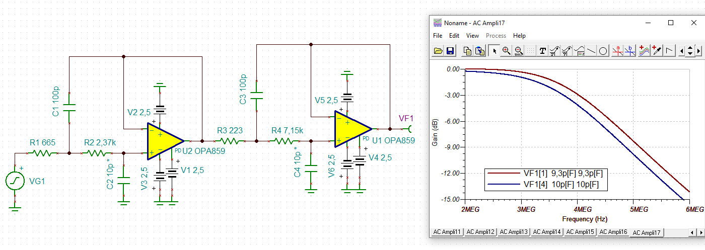
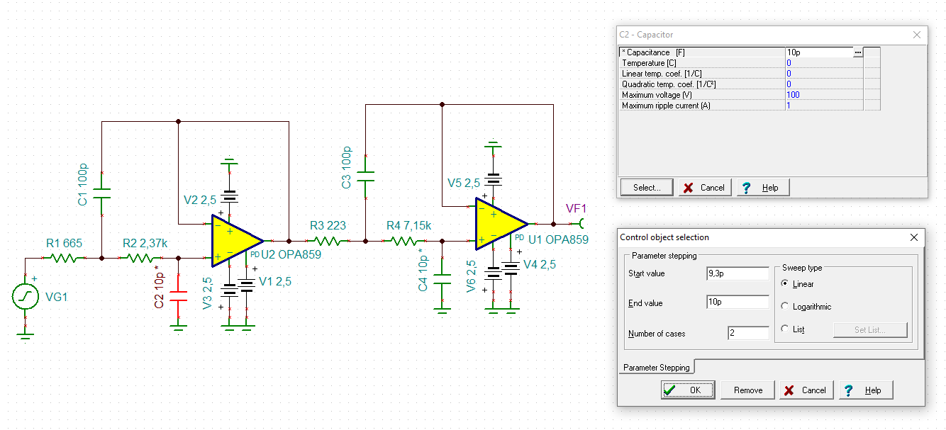
Other Parts Discussed in Thread: OPA659, OPA2810, OPA2822, OPA858, , TINA-TI

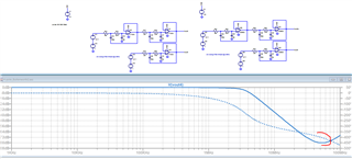
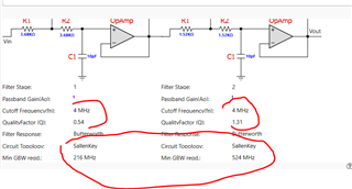
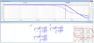
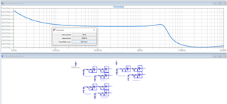
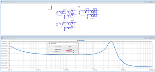
I used the TI Filter Design Tool to get a 4-pole Butterworth design using two Sallen & Key stages. Corner frequency was design at 4 MHz, yet the simulation shows -3dB at 3.4 MHz. Years ago Sallen & Key did not simulate well due to the positive feedback - I'm wondering if that is still the case. Also, I couldn't get TI PSpice to converge at all so I simulated in LTSpice with a similar amplifier. TI Spice file attached.

  • Nothing is attached, if you zip the LTSpice file and attach that, I can work with that also. Normally, 2 stages of MFB filter will work better. Also, that online filter tool does not try to pick the best fit parts for the requirements. Almost certainly the case a slower part will work,

  • Do MFB simulate better than Sallen & Key?

  • So actually I was after the LTSpice .asc file, I was not interested in working through PSpice for TI quite yet. I did try to open that file, and it tried - but never got there in the OrCad flow. 

  • Thanks Mark, yes that runs fine in LTSpice, notice the rising piece out at 100MHz, the SKF always suffers from worse stop band rejection than the MFB due to the feedthrough in the cap. 

    So to do this fresh, I would 1st use the old Filterpro tool to set the pole locations for 4th order Butterworth 

    Here that is showing the crazy high GBP built into that tool (and carried over to the current online TI tool)

    So easy to redo this in my MFB tool I developed for the Intersil online design tools, normally, I put the higher Q stages 1st to get lower integrated noise, and yes academia says the opposite to avoid clipping with the overshoot of that 1st stage. That is easy to avoid, but higher integrated noise is built in with ascending Q. 

    I calculate I need at least 50MHz GBP for this, but this is also using a GBP adjustment flow - I saw in the LTSPice file a 10V supply (the OPA659 cannot do that). I am kind of thinking maybe the OPA2810 would do, well my tool appears to be broken. Have to pick up later, but you could just try those ADI RC values with the OPA2810

  • Thanks for the info. But, alas - my predecessor at the company achieved 4-pole Butterworth response with 2 unity gain Sallen & Key structures and that's what the PCB currently is laid out for, hoping to get the correct R&C values for a 4 MHz corner. My hand analysis (via Excel) of the filter with unity gain Sallen & Key shows the TI filter solution (with the high-Q 2nd stage) works perfectly (the ADI design tool not so much, and it has the high-Q in the 1st stage), and this is the perfect math situation. I understand your concern on peaking, but right now I am focused on the corner frequency and less so on the stop band rejection. So I am wondering if this is more about the simulation not working when using the correct values when in reality the design works as desired for the corner frequency when built and tested? I understand the benefits of MFB structure, but I'd like to see how far I can get with Sallen & Key right now.

  • Ok, I got an older version of my  MFB working and there were more errors than I though in the newer one I opened. It is now reporting a min GBP of 240MHz. But, the SKF will allow current feedback solutions - if you only had a place for the feedback R. 

    So if you want a 10V supply unity gain stable VFA at about 250MHz BW, perhaps the OPA2822. 

    Now If you are calculating without considering the amp bandwdith, you may well get ideal results, but you won't in the board build. Somewhere I have a SKF design flowa that accounts for Bandwidth but I have not used it for a long time - the ADI tool allows you to adjust the RC for the amplifier BW, which may be what it is doing - just force that design to something about the same speed as the OPA2822 and find those RC values. The ADI solution flows a much more sophisticated than the TI tool based on the circa 1989 Filterpro solutions. 

  • I am calculating without the GBWP, but to me that only affect the stop band rejection provided you have significant enough gain to at least 10x your corner frequency limiting what I refer to as "ultimate rejection".

    But I still need to see if I can get the Sallen & Key structures to work, as mentioned above. I guess I'm asking - if the math says the corner is correct, would that also be the tested circuit performance but just not simulate well? I guess I'm trying to tie design equations vs simulation vs actual performance. Any thoughts?

  • There are many ways to go wrong on this, you need to include the V+ input C in setting your external input Cap -most of these higher speed parts like some loading at least 200ohm 

    And the actual shape always moves off from ideal op amp RC due to op amp bandwidth limits. 

  • Hi Mark,

    don't overlook the common mode input capacitance of OPA858 of 0.62pF. This adds to the 10pF filter capacitances. When I take it into consideration the frequency response becomes correct:

    mark_opa859.TSC

    Kai

  • Hi Kai,

    I had forgotten about that issue when using Sallen & Key structures at high frequency - you have to add in the input capacitance of the amplifier due to the small filter capacitance there. Let me try that. You attached a file - mark_opa859.TSC - what is that? I can't seem to open it.

    Also, I've had difficulty getting TI PSpice to run with this circuit - doesn't seem to converge - any ideas on how to make it run?

  • Hi Mark,

    Let me try that. You attached a file - mark_opa859.TSC - what is that? I can't seem to open it.

    Sorry, this is a file being created by TINA-TI. TINA-TI is free and can be downloaded here:

    https://www.ti.com/tool/TINA-TI

    TINA-TI is the former TI's simulation tool and shall be replaced by TI PSpice in the near future, if I'm not wrong.

    Also, I've had difficulty getting TI PSpice to run with this circuit - doesn't seem to converge - any ideas on how to make it run?

    Sorry, I'm not familiar with TI PSpice so far.

    Kai

  • Hi Kai,

    I moved over to TINA-TI and it is rather nice. I imported your .TSC and it runs well. One question - I was expecting one plot when I ask for AC Analysis/AC Transfer Characteristic but when I run it, it generates 4 plots rather than one and I haven't been able to figure out what the 4 plots present as they all reference VF1. Could you explain? Thanks.

  • Hi Mark,

    I have configured C2 and C4 as "control objects" and step them from 9.3pF to 10pF. This gives four curves. Go with the mouse pointer onto the curves and watch the message in the task bar at the bottom of TINA-Ti window.

    To configure a component as "control object" click on "Analysis" and "Select Control Object". Click on the component of question and click "...".

    If you don't want these control objects, delete C2 and C4 and take fresh capacitors.

    Kai

  • Hi Kai,

    Moving over the traces I do see how they are defined at the bottom of the schematic window. But it I wanted to modify the step parameters, how do I do that? How do I see what items are set to be control objects and what their parameters are? There doesn't seem to be a way to see the control objects already defined before running a sim. Any thoughts?

    Mark

  • Hi Mark,

    to see the parameters click again on "Analysis" and "Select Control Object". Then click on the component of question and click "...":

    Kai

  • Thanks, I saw that - but is there any way just looking at the schematic or the pull-downs to know which items are control objects? Or do you have to check every component?

  • Hello Mark,

    I am attaching TINA's documentation on Parameter Stepping; you may use the phrase 'Parameter Stepping' with CTRL+F to find the right place in the document.  

    ADVANCED TOPICS MANUAL.pdf

    In short, my experience has been such that most numerical parameters are allowed to be control objects and be stepped through, so to speak.

    I am also attaching a link to a TI video on control objects, just for posterity for those who may find this forum useful.  

    https://training.ti.com/sweeping-parameters-tina-titm-simulator

    Best,

    Alec

  • Thank you Alec,

    But to get back onto the original concept for this thread, I'm looking to find more info on how the circuit values are selected in your Filter Design Tool. For example - in this case I know I want a 4-pole Butterworth - that transfer function H(s) is well known. How do I get from that to the Rs & Cs in the Sallen & Key structures? I'm not looking for the inner workings of your design tool, just maybe a salient theoretical article on the method used. As a further example, your configuration is for the low-Q circuit in the first stage and the High-Q in the second, while Analog Devices has a filter design tool that does the opposite. Just wondering all the details that go into the design choices and process, over blindly using an on-line tool. Anything you can point me to would be greatly appreciated. Thanks.

  • The TI online tool is based on the much older FilerPro done by BurrBrown back around 1989. It is a very large area to get into, but you might find something in this document, r

    sbfa001c_filterpro users guide.pdf

    The academic pole sequencing is low to higher Q for clipping purposes. I (and apparently ADI) decided to flip that around to get lower integrated noise, here is an example app brief on this topic where I was using an ADI example to show the improvement possible, These are starting to dissappear from the web, but I have a copy of AN1580 here, 

    Testing Filter Designer for gain and Q sequencing AN1580.pdf

    And then I had published quite a lot on advanced filter design while at Interesil, here I found one, Here is a more detailed discussion, 

    https://www.edn.com/advanced-considerations-for-gain-and-q-sequencing-in-multistage-lowpass-active-filters/

    https://www.electronicdesign.com/archive/article/21791804/move-beyond-active-filter-design-mythology-to-improve-your-discrete-opampbased-designs

  • Hi Mark,

    the www is full of examples of 4-pole Butterworth filters. I prefer circuits with two identical resistors per stage and a gain of 1V/V. You can easily fetch a filter from the www and adapt it to your needs. This is no rocket science. And you always have the ability to simulate your circuit to see what's going on...

    Choose the cap values high enough so that the cap at the +input of OPAmp dominates the input capacitance of OPAmp. A 10pF filter capacitance in combination with a 1pF input capacitance is no good choice!

    Choose the resistors big enough so that the driving OPAmp has no issues with the driving current. You can easily check the flowing currents in the simulation.

    As a further example, your configuration is for the low-Q circuit in the first stage and the High-Q in the second, while Analog Devices has a filter design tool that does the opposite.

    What comes first doesn't matter in the very most cases. Both has its pros and cons. The high-Q circuit always shows a higer ringing and a bigger overshot. So, to prevent clipping the low-Q circuit is normally used in the first stage.

    But using the low-Q circuit in the second stage can give a lower noise, as Michael already mentioned.

    Kai

  • So Kai, as you come down into making an automated online design tool the 1st thing you discover is you are way underconstrained - literally an infinite range of RC combinations can hit the nominal filter target and any set of Q and gain sequencing can do a multistage shape. As you drill deeper, it is possible to hit that same target with better dynamic range and sensitivities if you work at it. This is essentially free dynamic range improvement in production, but not in design effort. 

    Have not looked at what is out there for some time, but I did run through some industry tool testing n these two articles some years back, 

    https://www.edn.com/testing-op-amp-tools-for-their-active-filter-design-accuracy-and-dynamic-range/

    https://www.edn.com/active-filter-design-tools-shootout/

  • So Mike - I was in the process of typing a reply when yours came in hitting the nail on the head. A second order system has a denominator in s, where the coefficients tell you Fc and Q. You can also use a Sallen & Key equation to match these with R1, R2, C1, C2, and K. So you have 2 equations with 5 unknowns. As you say - the situation is underconstrained. Simplifications can be done (equal Rs, equal Cs, unit gain, etc.) but each has a ramification. And I'm also not sure when you can say you can use a unity gain configuration vs when you can't. I'll read through the referenced papers, but if you have any more ideas on insights with these constraining concepts and ramifications, that is what I am looking for. Thanks.

    Mark

  • 6507.4-pole_Butterworth2.zip

    Attached is a .zip file of LTSpice sims of the ADI filter tool design vs TI filter design tool. I've used the LT1810 amplifier as that is what we had chosen previously - there is also a sim version using the ADI design with their AD8032 that was recommended (I think LT1810 is better). The design value for the cap at the amp input is 10 pF, but I used 8.2 pF standard value and let the amp input capacitance make up the rest. Also note - beneath each 4-pole circuit is just the second stage also simmed so I could look at each stage individually to see which one was peaking, etc. I think the TI filter design performed better, most noticeably ay stop band rejection. This is what I was referring to - how do you select Rs & Cs for the best design?

  • Ok Mark, I assumed the design tool delivered 10pF at the V+ input, here I adjusted the LT1810 versions to back out the 2pF it has (8pF on each V+ input) and probed just those 4th order outputs, pretty identical at cutoff for the ADI and TI RC selections. And yes, the TI higher R's (more noise) had better stop band

    here I ran the output noise for the ADI LT1810 4th order, Integrated to 192uVrms

    And then for the TI values using the LT1810, and yes, this is what you get with the higher Q last, 225uVrms - not a big change, but the earlier ADI one was like free SNR improvement for the same 4th order shape. 

  • So you are saying the ADI design had somewhat lower noise at the expense of stopband rejection, correct? OK, but what keeps getting glossed over is: How did the selection on Rs & Cs take place for either design?

  • There is no such thing as an optimum solution, just tradeoffs. 

    The simplest designs go equal R or C to get rid of degrees of freedom, those are in textbooks. 

    More sophisticated ones scale the total R's to not increase the in band noise too much then look for ratios that will reduce the noise gain peaking inside the filter and then work on min allowed GBP and R adjustments for the device selected . Not much of that is published and I know my spreadsheets are very confidential - I suspect ADI's are as well. I did just find my Intersil one, have not looked at for years, but putting 4MHz gain of 1 and Q=1.41 tells me I need at least 55Mhz GBP, kind of consistent with the 80MHz part the ADI tool selected and quite a lot lower than the old filterpro tool. Remember, excess GBP to hit the filter shape is excess mW. 

  • I think I found what I'm looking for in your SLOA049B app note. Section 4 (Math Review) maps the coefficients into Q and FSF, and then those are used in the later sections to help derive the values, also with the "m" and "n" factors in Appendix A for the simplifications. I get it that there is proprietary algorithms built into filter design tools, but this document was what I was looking for - to know what was being optimized. I also understand there are other things like stopband rejection and noise reduction inherent in specific architectures and circuit arrangements.