This thread has been locked.

If you have a related question, please click the "Ask a related question" button in the top right corner. The newly created question will be automatically linked to this question.

INA211: Spice simulation/application questions (INA211BIDCKR)

Part Number: INA211
Other Parts Discussed in Thread: INA210-215EVM, INA190, INA186

Hi,

I have a few questions concerning the INA211 current sense amplifier.

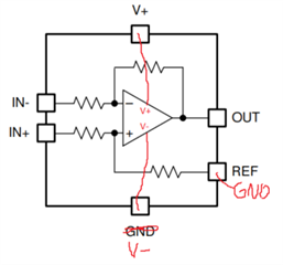
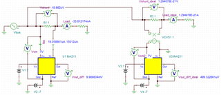
First, I am assuming here that the GND pin is the negative rail voltage pin of the op-amp (see attached drawing). If it is the case, why isn’t the GND pin called something like V-? Still assuming that GND is for the negative rail, in an application where I need to sense a sinewave (alternating current), can I put the GND pin to the negative supply of a bipolar source, like it my example below? That way my output voltage can be bipolar, which is what I want ideally.

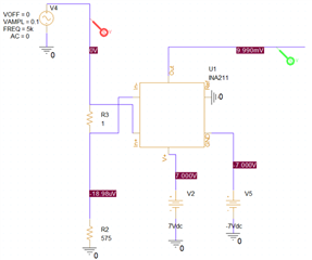
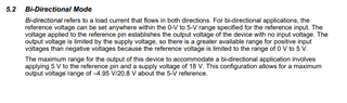
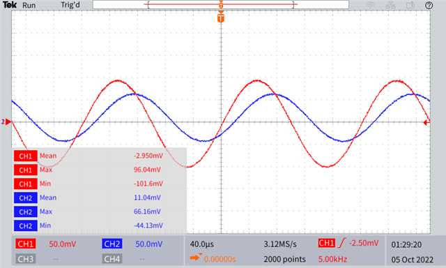
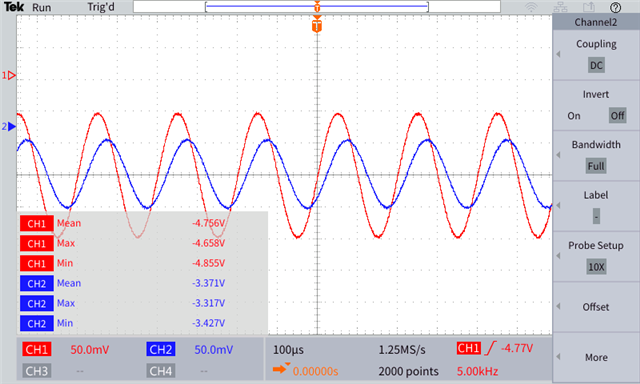
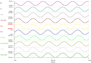
In the datasheet we can read that in order to work in a “bidirectional configuration”, the REF pin should be connected to a reference voltage and that the output voltage is going to be biased upwards by that reference level, but when I do so (in Pspice), everything goes well when my current flows from IN+ to IN- but in the opposite direction, the output voltage offset as well as the gain is very strange (I can’t make sense of it).

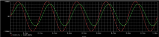
My last question is: What does a “bi-directional” current sense amplifier means? Does it only mean that the component can be used in a High-side or Low-side configuration? Or does it mean current can flow both ways, meaning I can sense alternating current that goes below and above my reference, which is GND? Because if it is the case, the Pspice simulation suggests otherwise.

I hope I explained it well enough, I can provide more details if needed.

Thanks in advance,

  • Hello Jerome,

    I am looking this over and will respond shortly.

    Best,

    Peter

  • Yes. The GND pin is technically connected to the V- of the internal amplifier. The main reason this pin is called GND is because these devices are usually designed with low, single-ended supply voltage; however, it is still valid to power them with a dual positive and negative supply as long as you make sure to not violate the input Vcm rating. You will want to use best practice power sequencing also, so power up the GND pin (V-) first, then the Vs pin (V+), or at least simultaneously.

    Whenever the GND pin is not biased to system ground (0V), then the equation for Vout becomes:

    Vout = Vgnd_csa + Vbias + Vsense*Gain,

    Where Vbias = Vref – Vgnd_csa. Usually Vgnd_csa = system ground = 0V.

    Keep in mind the PSPICE measures nodes single-ended to Earth ground (0V). So in your circuit Vout is:

    Vout = -7V + (0V- -7V) + Vsense*Gain = 0V + Vsense*Gain

    This matches up with the data plot you have attached. The bias of the output voltage is at 0V, it is centered across Earth ground because REF = Earth ground.

    For your last question. Bi-directional means the device can measure positive and negative currents, thus bi-directional devices have REFERENCE pins to bias the output to a mid-level voltage. The pspice simulation appears to be illustrating this behavior.

    Hope this helps. Please post back with any other questions you may have.

    Sincerely,

    Peter

  • Hi,

    Thanks for your detailed answer. You made it clear how it is supposed to behave.

    Concerning the strange output waveform I was talking about, if you look carefully at the green waveform in my previous post, you can see that the negative peaks are distorted when comparing them to the positive peaks which are not distorted (if we compare it to the red sinewave). What explains that? Out of curiosity, I tried changing the DC offset to see what happens and it seems like at one point, when the DC offset is high enough, those negative peaks become normal. Again, all of this has only been observed in simulations.

    Concerning the bias of the output voltage at 0v (or almost since there is a small expected 35uA input bias current) in the plot I attached, yes you are right.

    Lastly, I saw something pretty confusing in the datasheet of the evaluation board for that part (INA210-215EVM). It is stated that the "reference voltage can be set anywhere within the 0v to 5v range specified for the reference input", which would mean I can't put my gnd lower than -5V if my REF is at 0v. Is that really it?

    I hope I explained it well enough.

    Best regards,

    Jerome

  • Hey Jerome,

    I think I see what you are referring to at the negative peaks. Maybe it could be changing input bias currents due to oscillating input Vcm? Looking at the plot below, you can refer to the red curve (Vref=Vs/2and the drastic transition of IB when Vcm ~ Vs/2. This is the same as your circuit. Vs = 14V, Vref = 7V and Vcm = Vref +/-100mV. But maybe something else could be going on. I would need to see more data.

    I would disregard that text from the EVM User's Guide. According to the datasheet, Vref can be anywhere in between GND and Vs and Vs can be up to 26V. I believe this text is a partial typo from another user's guide and I will look into correcting this. Sorry for the inconvenience. 

    Sincerely,

    Peter

  • Hi,

    I confirm that this also happens in real life. What bugs me is the fact that it is inconsistent and I cannot make sense of it and compute it. It could be due to the oscillating input Vcm affecting the input bias current as you say, but isn't the input bias current supposed to be neglectable given how small it is (micro amps)?

    When just applying DC, the offset is there and it is in the order of millivolts (seems like the larger the current through the shunt, the larger it is) so my question is: how can an input bias current in the order of uA lead to an offset voltage in the order of millivolts in the output signal? Isn't it the input offset current that can lead to a voltage offset?

    If I remember well, the voltage offset caused by the input offset current can be obtained from V = Input offset current * gain * input impedance?

    Lastly, I understand that the input offset voltage (Vo) is the voltage needed in order to output 0V. If it is said in the datasheet that it is of 35uV, does that mean at 36uV, it will output 0.5mV (1uV*500=0.5mV) or will 36uV output 18mV (36uV*500=18mV)?

    Again all of those offsets are pretty small compared to the offsets I observed.

    Best regards,

    Jerome

  • INA211_floating.TSC

    Hey Jerome,

    Any more schematic information would be helpful, but I think the issue is simply you are measuring very small current (hundreds of µA) and thus offset error from IB (~19µA) will become substantial. The offset is generated because IB flowing into IN- pin is also flowing across the shunt resistor of 1-Ω, which creates ~19µV of offset. Multiply this by 500V/V and this yields 9.5mV of output referred offset just from the IB and the 1-Ω resistor.

    Here is a simulation of the circuit you sent initially and also another circuit which is the same except I buffer the shunt voltage with ideal voltage source to simulate if INA211 had ideal input resistance. You can clearly see how the output is shifted by +10mV due to Vos_IB. Keep in mind that offset could be worse because initial offset (Vosi) starts at 35uV max (17.5mV output with INA211). There could be up to 2.8uV of offset due to DC CMRR ((12-7)*10^(-105dB/20)). Then you will also have variable offset from AC CMRR. At 5kHz, CMRR drops down to ~90dB typical according to figure 9 of datasheet.

    The last non-ideality is that it is entirely possible is that the IB values are drastically changing (for example IB = +19uA when Vbus = 0.1V and 0uA when Vbus =-0.1V. See Figure 11 of datasheet which I show below. This would introduce even more non-linearity to the measurement. I would try measuring IB-/IB+ in your realistic test setup. You can do this by inserting small input resistors in between Vshunt and V_IN+ and V_IN- and then measure the voltage drops across them while Vbus is oscillating. The current INA211 model (using the attached simulation circuit) behaves such that this drastic change in IB (crossover region) occurs when Vbus = -4.859V, as opposed to 0V = Vs/2=Vref, which I would deduce based upon Figure 11. 

    Overall, it is difficult to precisely measure smaller currents (<1mA) with the INA21x or other relatively low-input impedance amplifiers with IB in the uA range. On top to this, non-linearity can be introduced due to the oscillating input common-mode voltage (Vcm), partially due to AC CMRR, but also due to the potential that Vcm could be oscillating about the IB crossover region.

    From our current-sense amplifier portfolio, I would either recommend the INA296 or the INA190A5/INA186A5. The INA296 is not a high-input impedance device, but the cross over region should be way below your circuit's Vcm. The device also has much better AC and DC CMRR and offset specifications. The INA190/INA186 are high-input impedance devices with common-mode IB <3nA. The downside is that max recommended supply voltage is <5.5V so at best you would supply device with Vs=2.25V and GND=-2.25V and this would add more power circuitry and reduce dynamic range.

    To understand better how I made my offset calculations, please refer to our training videos. The op amp and instrumentation amplifier videos are valid too.

    https://training.ti.com/ti-precision-labs-amplifiers?context=1139745

    Sincerely,

    Peter